LX2202CLQ データシートの表示(PDF) - Microsemi Corporation
部品番号
コンポーネント説明
メーカー
LX2202CLQ Datasheet PDF : 12 Pages
| |||
LX2202
TM
® 2A Li-Ion Linear Charger and Power Control
PRODUCTION DATA SHEET
ABSOLUTE MAXIMUM RATINGS
Supply Voltage (VUSB or VDD ) ..........................................................-0.3V to 7V
Analog Input Signals (VIDx, VM, SNS) .............................................-0.3V to 7V
Battery Charging Current (IBAT).........................................................................2A
Discharge Current (IVDD)....................................................................................3A
Operating Junction Temperature.................................................................. 150°C
Storage Temperature Range...........................................................-65°C to 150°C
USB Maximum DC Current .......................................................................500mA
USB Maximum Surge Current...........................................................................2A
RoHS / Pb-free Peak Package Solder Reflow Temperature
(40 second maximum exposure) ...................................................... 260°C(+0, -5)
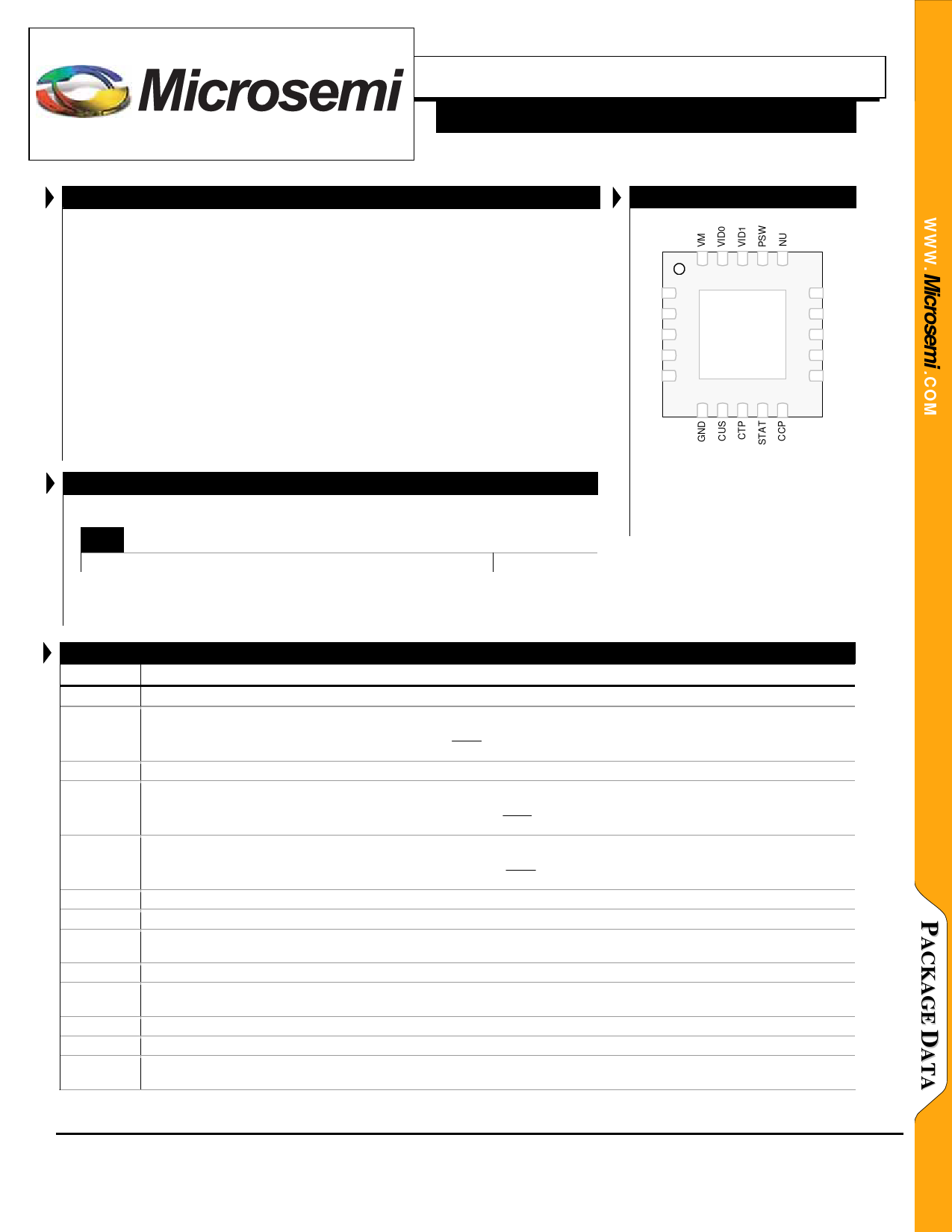
PACKAGE PIN OUT
VDD
VDD
VDD
VDD
USB
20 19 18 17 16
1
15
2
14
3
13
4
12
5
Pad Is GND 11
6 7 8 9 10
NU
BAT
BAT
BAT
CMP
Note: Exceeding these ratings could cause damage to the device. All voltages are with respect to
Ground. Currents are positive into, negative out of specified terminal.
THERMAL DATA
LQ Plastic Micro Lead Frame Quad Package 20-Pin
THERMAL RESISTANCE-JUNCTION TO AMBIENT, θJA
40°C/W
Junction Temperature Calculation: TJ = TA + (PD x θJA).
The θJA numbers are guidelines for the thermal performance of the device/pc-board system. All of the
above assume no ambient airflow.
LQ PACKAGE
(Top View)
RoHS / Pb-free 100% Matte Tin Lead Finish
Name
BAT
CCP
CMP
CTP
CUS
GND
NU
PSW
VDD
VIDx
USB
VM
STAT
FUNCTIONAL PIN DESCRIPTION
Description
Charging Output - This pin is wired to the positive terminal of the battery. (The negative battery terminal is wired to GND.)
Charge Current Programming Pin - A resistor (RCP) is connected between this pin and GND. The constant current is
determined
by
the
following
relationship:
IBAT(MAX)
=
73200
R CCP
Compensation Pin – Connect a 0.1µF compensation capacitor from this pin to VDD.
Charge Termination Programming Pin – A resistor (RTP) is connected between this pin and GND. The termination charge
current
is
determined
by
the
following
relationship:
IBAT(MIN)
=
5250
R CTP
Maximum USB Current Programming Pin – A resistor (RUS) is connected between this pin and GND. The Hi Level charge
current
is
determined
by
the
following
relationship:
IUSB(HIGH)
=
1211
R USB
Common Ground
This pin is floating and will not affect performance.
PMOS Switch driver – This output is designed to drive the gate of an external PMOS power switch. The driver is pulled low
(PMOS on state) when VDD > VBAT.
Common Power Node – Connects to system power bus.
State Select Input – Applying a two bit TTL compatible signal sets the desired state of the charger corresponding to the Truth
Table.
Voltage Input – Current limited USB input. Apply a USB compliant power input.
Voltage Mode Select - Selects the constant voltage charge level. Wired to USB for 4.1V and GND for 4.2V.
Status - This pin is a logic high level when the battery is being charged. A low signal indicates either under voltage lockout,
charge completed, or VBAT > VDD, or VID0 = VID1 = 0.
Copyright © 2004
Rev. 1.0a, 2006-02-09
Microsemi
Integrated Products Division
11861 Western Avenue, Garden Grove, CA. 92841, 714-898-8121, Fax: 714-893-2570
Page 2
Share Link: 