MAX1211(2003) データシートの表示(PDF) - Maxim Integrated
部品番号
コンポーネント説明
メーカー
MAX1211 Datasheet PDF : 29 Pages
| |||
19-2922; Rev 0; 8/03
EVAALVUAAILTAIOBNLEKIT
65Msps, 12-Bit, IF Sampling ADC
General Description
The MAX1211 is a 3.3V, 12-bit analog-to-digital convert-
er (ADC) featuring a fully differential wideband track-
and-hold (T/H) input, driving the internal quantizer. The
MAX1211 is optimized for low power, small size, and
high dynamic performance in intermediate frequency
(IF) sampling applications. This ADC operates from a
single 3.0V to 3.6V supply, consuming only 358mW
while delivering a typical signal-to-noise ratio (SNR) per-
formance of 66dB at an input frequency of 175MHz. The
T/H driven input stage accepts single-ended or differen-
tial inputs. In addition to low operating power, the
MAX1211 features a 13mW power-down mode to con-
serve power during idle periods.
A flexible reference structure allows the MAX1211 to
use its internal precision bandgap reference or accept
an externally applied reference.
The MAX1211 supports both a single-ended and differ-
ential input clock drive. Wide variations in the clock
duty cycle are compensated with the ADC’s internal
duty-cycle equalizer.
The MAX1211 features parallel, CMOS-compatible out-
puts. The digital output format is pin selectable to be
either two’s complement or Gray code. A separate
power input for the digital outputs accepts a voltage
from 1.7V to 3.6V for flexible interfacing with various logic
levels. The MAX1211 is available in a 6mm x 6mm x
0.8mm, 40-pin thin QFN package with exposed paddle
(EP), and is specified for the extended industrial (-40°C
to +85°C) temperature range.
Applications
IF and Baseband Communication Receivers
Cellular, LMDS, Point-to-Point Microwave,
MMDS, HFC, WLAN
Ultrasound and Medical Imaging
Portable Instrumentation
Low-Power Data Acquisition
Features
o Direct IF Sampling Up to 400MHz
o Excellent Dynamic Performance
66dB SNR at fIN = 175MHz
76dBc SFDR at fIN = 175MHz
o Differential or Single-Ended Clock
o 3.3V Low-Power Operation
358mW (Differential Clock Mode)
327mW (Single-Ended Clock Mode)
o Accepts 20% to 80% Clock Duty Cycle
o Fully Differential or Single-Ended Analog Input
o Wide ±1VP-P Differential Analog Input Voltage
Range
o 700MHz Input Bandwidth
o Power-Down Mode
o CMOS-Compatible Outputs in Two’s Complement
or Gray Code
o Out-of-Range and Data Valid Indicators
o Small, 40-Pin Thin QFN Package with Exposed
Paddle
o Evaluation Kit Available (Order MAX1211EVKIT)
Ordering Information
PART
TEMP RANGE PIN-PACKAGE
MAX1211ETL -40°C to +85°C 40 Thin QFN 6mm x 6mm
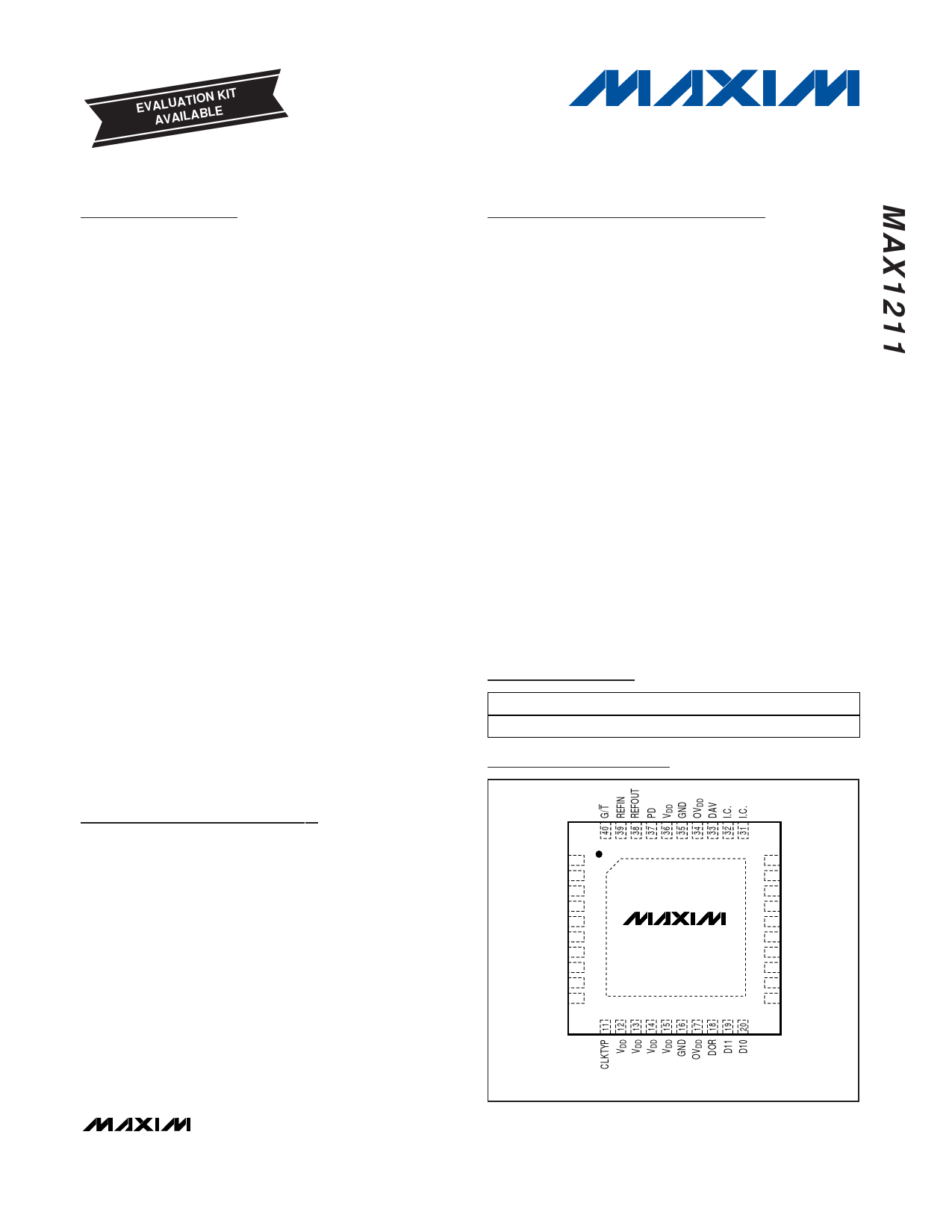
Pin Configuration
TOP VIEW
REFP 1
REFN 2
COM 3
GND 4
INP 5
INN 6
GND 7
VDD 8
CLKN 9
CLKP 10
MAX1211
EXPOSED PADDLE (GND)
30 D0
29 D1
28 D2
27 D3
26 D4
25 D5
24 D6
23 D7
22 D8
21 D9
THIN QFN
6mm × 6mm × 0.8mm
________________________________________________________________ Maxim Integrated Products 1
For pricing, delivery, and ordering information, please contact Maxim/Dallas Direct! at
1-888-629-4642, or visit Maxim’s website at www.maxim-ic.com.
Share Link: 