MAX1211ETL(2003) データシートの表示(PDF) - Maxim Integrated
部品番号
コンポーネント説明
メーカー
MAX1211ETL Datasheet PDF : 29 Pages
| |||
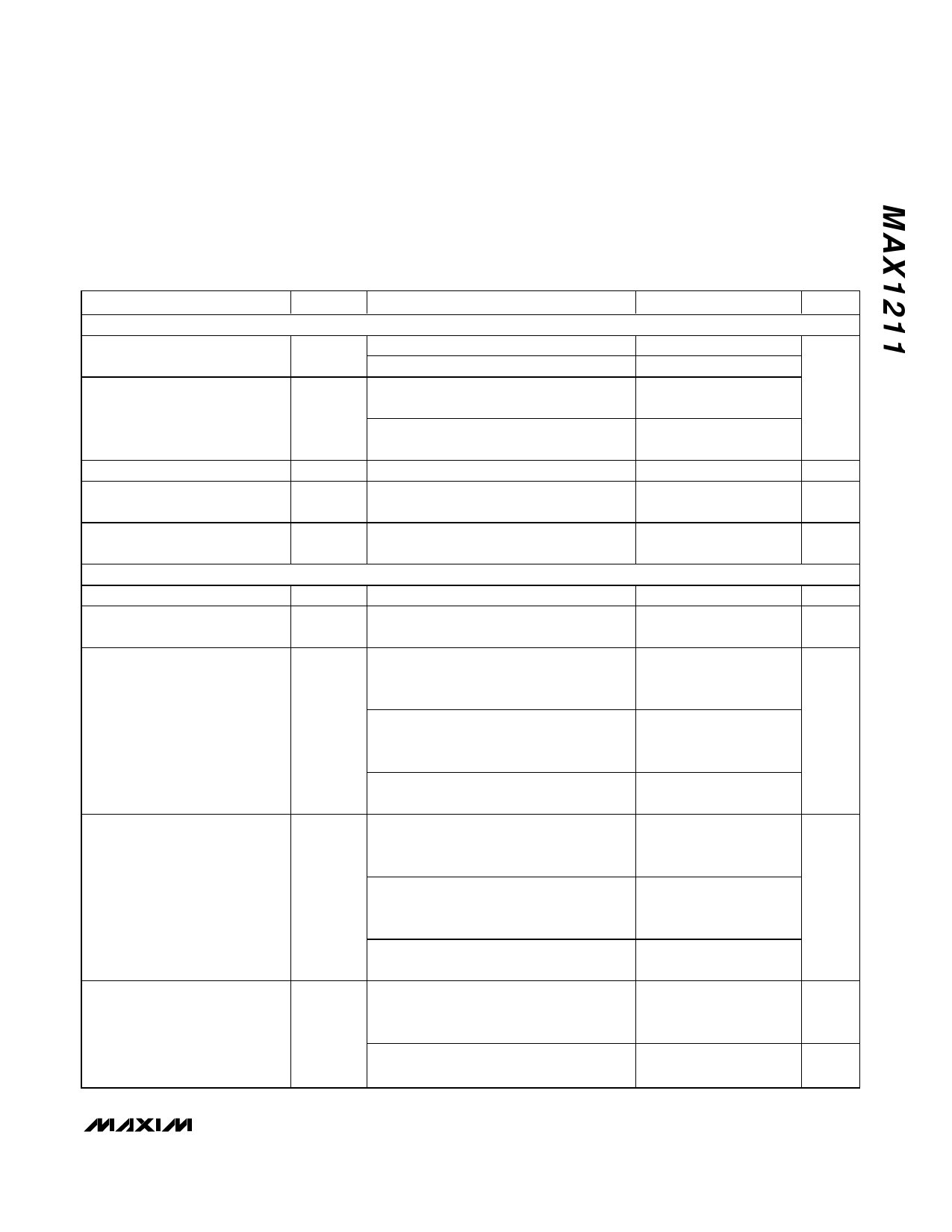
65Msps, 12-Bit, IF Sampling ADC
ELECTRICAL CHARACTERISTICS (continued)
(VDD = 3.3V, OVDD = 2.0V, GND = 0, REFIN = REFOUT (internal reference), CREFOUT = 0.1µF, CL ≈ 5pF at digital outputs, VIN =
-0.2dBFS, CLKTYP = high, PD = low, G/T = low, fCLK = 65MHz (50% duty cycle), CREFP = CREFN = 0.1µF to GND, 10µF between
REFP and REFN, CCOM = 0.1µF in parallel with 2.2µF to GND, TA = -40°C to +85°C, unless otherwise noted. Typical values are at TA
= +25°C.) (Note 1)
PARAMETER
D11–D0, DOR Tri-State Output
Capacitance
DAV Tri-State Output
Capacitance
POWER REQUIREMENTS
Analog Supply Voltage
Digital Output Supply Voltage
SYMBOL
COUT (Note 2)
COUT (Note 2)
CONDITIONS
VDD
OVDD
Normal operating mode,
fIN = 32.4MHz at -0.2dBFS,
CLKTYP = GND, single-ended clock
MIN TYP MAX UNITS
3
pF
6
pF
3.0
3.3
3.6
V
1.7
2.0
VDD
V
+ 0.3V
99
Analog Supply Current
IVDD
Normal operating mode,
fIN = 32.4MHz at -0.2dBFS,
CLKTYP = OVDD, differential clock
Power-down mode; clock idle,
PD = OVDD
Normal operating mode,
fIN = 32.4MHz at -0.2dBFS,
CLKTYP = GND, single-ended clock
mA
108
121
4
12
327
Analog Power Dissipation
Digital Output Supply Current
PDISS
IOVDD
Normal operating mode,
fIN = 32.4MHz at -0.2dBFS,
CLKTYP = OVDD, differential clock
Power-down mode, clock idle,
PD = OVDD
Normal operating mode,
fIN = 32.4MHz at -0.2dBFS,
OVDD = 2.0V, CL ≈ 5pF
Power-down mode; clock idle,
PD = OVDD
mW
358
400
13
40
10
mA
19
µA
_______________________________________________________________________________________ 5
Share Link: 