MAX17491 データシートの表示(PDF) - Maxim Integrated
部品番号
コンポーネント説明
メーカー
MAX17491 Datasheet PDF : 12 Pages
| |||

Single-Phase Synchronous MOSFET Driver
ABSOLUTE MAXIMUM RATINGS
VDD to GND...............…………………….………….. -0.3V to +6V
SKIP to GND..................………………………………-0.3V to +6V
PWM to GND ................……………………………….-0.3V to +6V
DL to GND ..................................................-0.3V to (VDD + 0.3V)
BST to GND ............................................................-0.3V to +36V
DH to LX ....................................................-0.3V to (VBST + 0.3V)
BST to VDD .............................................................-0.3V to +30V
BST to LX ................…………………………………...-0.3V to +6V
Continuous Power Dissipation
8-Pin 3mm x 3mm TQFN
(derate 23.8mW/°C above +70°C) .............................1904mW
Operating Temperature Range .........................-40°C to +105°C
Junction Temperature ......................................................+150°C
Storage Temperature Range .............................-65°C to +150°C
Lead Temperature (soldering, 10s) .................................+300°C
Soldering Temperature (reflow) .......................................+260°C
Stresses beyond those listed under “Absolute Maximum Ratings” may cause permanent damage to the device. These are stress ratings only, and functional
operation of the device at these or any other conditions beyond those indicated in the operational sections of the specifications is not implied. Exposure to
absolute maximum rating conditions for extended periods may affect device reliability.
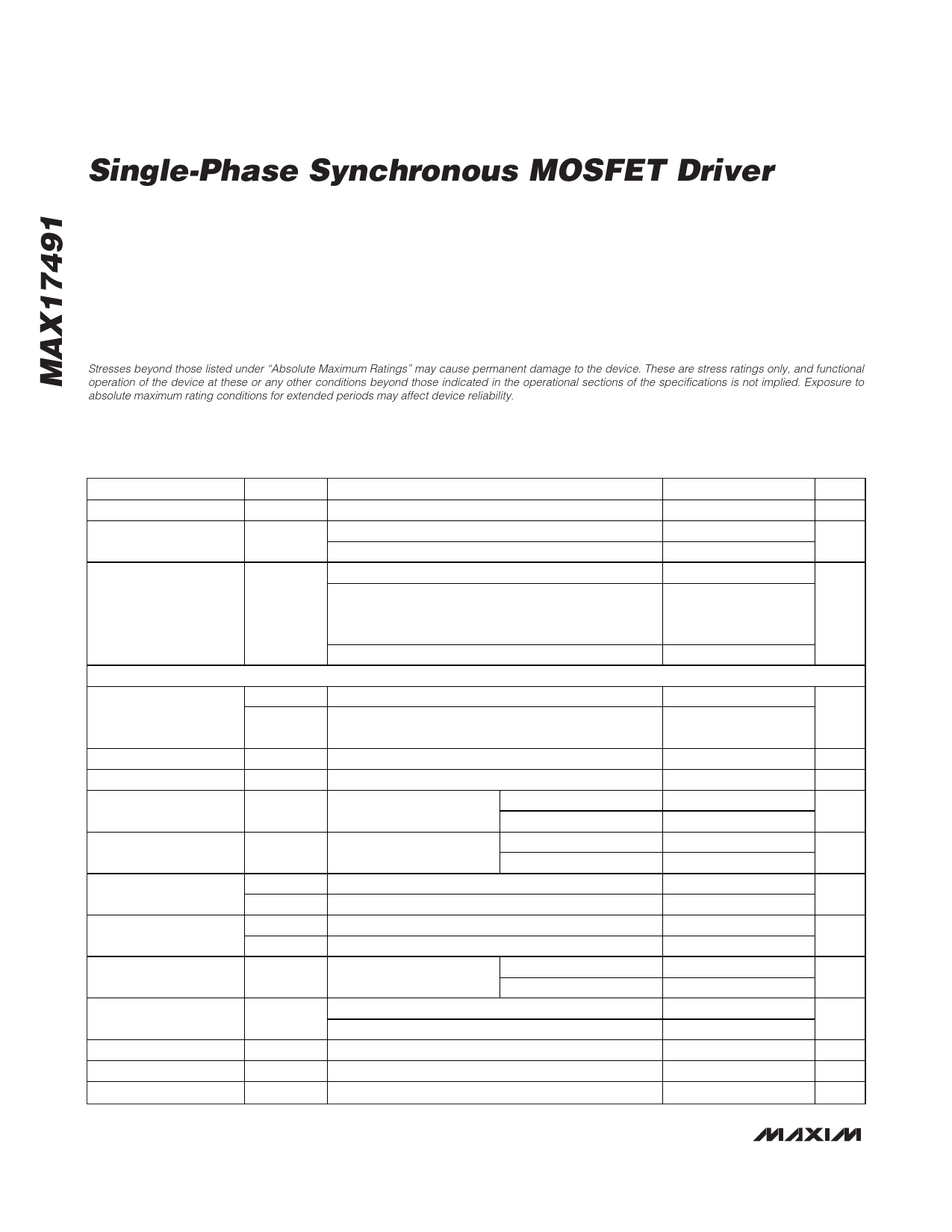
ELECTRICAL CHARACTERISTICS
(Circuit of Figure 1, VDD = VSKIP = 5V, TA = -40°C to +105°C, unless otherwise noted. Typical values are at TA = +25°C.) (Note 1)
PARAMETER
Input Voltage Range
VDD Undervoltage-
Lockout Threshold
SYMBOL
CONDITIONS
VDD
Rising edge, PWM disabled below this level
VUVLO(VDD)
Falling edge, PWM disabled below this level
PWM = open; after the shutdown hold time has expired
MIN
4.20
3.30
TYP
3.7
3.40
0.08
MAX
5.50
4.05
3.75
0.20
UNITS
V
V
Quiescent Supply
Current (VDD)
SKIP = GND, PWM = GND, LX = GND (after zero
IDD
crossing); this state should be equivalent to low-
power standby if LX = GND
0.15 0.30 mA
DRIVERS
PWM Pulse Width
SKIP = GND or VDD, PWM = VDD, VBST = 5V
tON(MIN)
tOFF(MIN)
Minimum on-time
Minimum off-time; required to allow the zero-crossing
comparator time to settle to the proper state
0.35 0.70
50
ns
300
DL Propagation Delay
tPWM-DL PWM high-to-DL low
15
ns
DH Propagation Delay
tPWM-DH PWM low-to-DH low
17
ns
DL-to-DH Dead Time
tDL-DH DL falling to DH rising
TA = 0°C to +85°C
10
ns
TA = -40°C to +105°C
10
DH-to-DL Dead Time
tDH-DL DH falling to DL rising
TA = 0°C to +85°C
10
ns
TA = -40°C to +105°C
10
DL Transition Time
tF_DL
tR_DL
Falling, 3.0nF load
Rising, 3.0nF load
10
ns
12
DH Transition Time
DH Driver
On-Resistance
tF_DH
tR_DH
RON(DH)
Falling, 3.0nF load
Rising, 3.0nF load
BST - LX forced to 5V
DH, high state (pullup)
DH, low state (pulldown)
8
ns
10
0.9 2.5
0.7 2.1
DL Driver
On-Resistance
RON(DL)
DL, high state (pullup)
DL, low state (pulldown)
0.7 1.6
0.3 0.9
DH Driver Source Current IDH_SOURCE DH forced to 2.5V, BST - LX forced to 5V
2.2
A
DH Driver Sink Current
IDH_SINK DH forced to 2.5V, BST - LX forced to 5V
2.7
A
DL Driver Source Current IDL_SOURCE DL forced to 2.5V
2.7
A
2 _______________________________________________________________________________________