MAX17491 データシートの表示(PDF) - Maxim Integrated
部品番号
コンポーネント説明
メーカー
MAX17491 Datasheet PDF : 12 Pages
| |||
Single-Phase Synchronous MOSFET Driver
VDD
BST
PWM
DRV
DH
DRIVER LOGIC
THERMAL SHUTDOWN
AND
LX
DEAD-TIME
CONTROL
UVLO
DRV#
VDD
SKIP
DL
LX
GND
ZX DETECTION
PAD
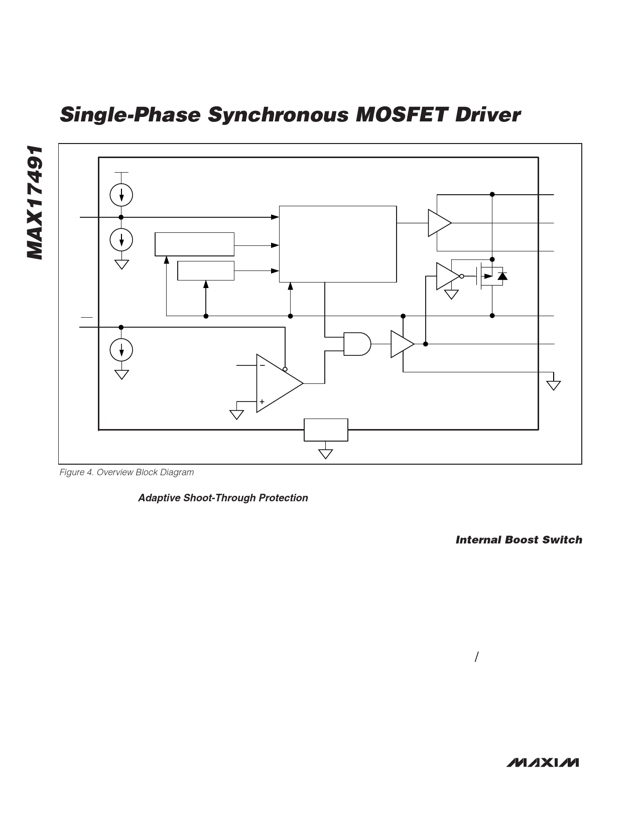
Figure 4. Overview Block Diagram
Adaptive Shoot-Through Protection
The DH and DL drivers are optimized for driving moder-
ately sized high-side and larger low-side power
MOSFETs. This is consistent with the low duty factor
seen in the notebook CPU environment, where a large
VIN - VOUT differential exists. Two adaptive dead-time
circuits monitor the DH and DL outputs and prevent the
opposite-side FET from turning on until the other is fully
off. The MAX17491 constantly monitors the low-side dri-
ver output (DL) voltage, and only allows the high-side
driver to turn on only when DL drops below the adap-
tive threshold. Similarly, the controller monitors the
high-side driver output (DH) and prevents the low side
from turning on until DH falls below the adaptive thresh-
old before allowing DL to turn on.
The adaptive driver dead time allows operation without
shoot-through with a wide range of MOSFETs, minimiz-
ing delays and maintaining efficiency. There must be a
low-resistance, low-inductance path from the DL and
DH drivers to the MOSFET gates for the adaptive dead-
time circuits to work properly; otherwise, the sense cir-
cuitry in the MAX17491 interprets the MOSFET gates as
off while charge actually remains. Use very short, wide
traces (50 mils to 100 mils wide if the MOSFET is 1in
from the driver).
Internal Boost Switch
The MAX17491 uses a bootstrap circuit to generate the
necessary drive voltage to fully enhance the high-side
n-channel MOSFET. The internal p-channel MOSFET
creates an ideal diode, providing a low voltage drop
between VDD and BST.
The selected high-side MOSFET determines appropriate
boost capacitance values (CBST in Figure 1), according
to the following equation:
CBST = QGATE ΔVBST
where QGATE is the total gate charge of the high-side
MOSFET and ΔVBST is the voltage variation allowed on
the high-side MOSFET driver. Choose ΔVBST = 0.1V to
0.2V when determining CBST. The boost flying capacitor
should be a low equivalent-series resistance (ESR)
ceramic capacitor.
8 _______________________________________________________________________________________
Share Link: 