MAX3030ECSE гғҮгғјгӮҝгӮ·гғјгғҲгҒ®иЎЁзӨәпјҲPDFпјү - Maxim Integrated
йғЁе“Ғз•ӘеҸ·
гӮігғігғқгғјгғҚгғігғҲиӘ¬жҳҺ
гғЎгғјгӮ«гғј
MAX3030ECSE Datasheet PDF : 14 Pages
| |||
Вұ15kV ESD-Protected, 3.3V Quad
RS-422 Transmitters
ABSOLUTE MAXIMUM RATINGS
(All Voltages Are Referenced to Device Ground, Unless
Otherwise Noted)
VCC ........................................................................................+6V
EN1&2, EN3&4, EN, EN............................................-0.3V to +6V
DI_ ............................................................................-0.3V to +6V
DO_+, DO_- (normal condition) .................-0.3V to (VCC + 0.3V)
DO_+, DO_- (power-off or three-state condition).....-0.3V to +6V
Driver Output Current per Pin.........................................Вұ150mA
Continuous Power Dissipation (TA = +70В°C)
16-Pin SO (derate 8.70mW/В°C above +70В°C)..............696mW
16-Pin TSSOP (derate 9.40mW/В°C above +70В°C) .......755mW
Operating Temperature Ranges
MAX303_EC_ ......................................................0В°C to +70В°C
MAX303_EE_ ...................................................-40В°C to +85В°C
Junction Temperature ......................................................+150В°C
Storage Temperature Range .............................-65В°C to +160В°C
Lead Temperature (soldering, 10s) .................................+300В°C
Stresses beyond those listed under вҖңAbsolute Maximum RatingsвҖқ may cause permanent damage to the device. These are stress ratings only, and functional
operation of the device at these or any other conditions beyond those indicated in the operational sections of the specifications is not implied. Exposure to
absolute maximum rating conditions for extended periods may affect device reliability.
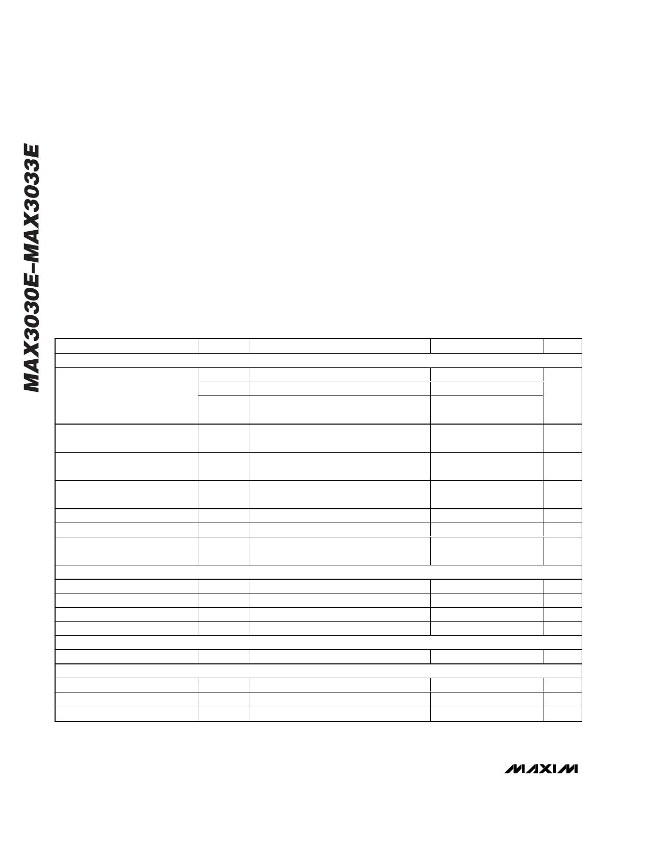
DC ELECTRICAL CHARACTERISTICS
(3V вүӨ VCC вүӨ 3.6V, TA = TMIN to TMAX, unless otherwise noted. Typical values are at VCC = +3.3V and TA = +25В°C.) (Note 1)
PARAMETER
DRIVER OUTPUT: DO_+, DO_-
Differential Driver Output
SYMBOL
CONDITIONS
VOD1
VOD2
VOD3
RL = 100в„Ұ, Figure 1
RL = вҲһ, Figure 1
RL = 3.9kв„Ұ (for compliance with V.11),
Figure 1
MIN TYP MAX UNITS
2.0
3.6
V
3.6
Change in Differential Output
Voltage
вҲҶVOD RL = 100в„Ұ (Note 2)
-0.4
+0.4
V
Driver Common-Mode Output
Voltage
VOC RL = 100в„Ұ, Figure 1
3
V
Change in Common-Mode
Voltage
Three-State Leakage Current
Output Leakage Current
Driver Output Short-Circuit
Current
INPUTS: EN, EN, EN1&2, EN3&4
Input High Voltage
Input Low Voltage
Input Current
Hot-Swap Driver Input Current
SUPPLY CURRENT
Supply Current
THERMAL PROTECTION
Thermal-Shutdown Threshold
Thermal-Shutdown Hysteresis
ESD Protection DO_
вҲҶVOC
IOZ
IOFF
ISC
VIH
VIL
ILEAK
IHOTSWAP
ICC
TSH
RL = 100в„Ұ (Note 2)
VOUT = VCC or GND, driver disabled
VCC = 0V, VOUT = 3V or 6V
VOUT = 0V, VIN = VCC or GND
(Note 3)
EN, EN, EN1&2, EN3&4 (Note 4)
No load
Human Body Model
-0.4
-150
+0.4
V
Вұ10
ВөA
20
ВөA
mA
2.0
V
0.4
V
Вұ2
ВөA
Вұ200
ВөA
100
ВөA
160
В°C
10
В°C
Вұ15
kV
2 _______________________________________________________________________________________
Share Link: 