MAX4613 データシートの表示(PDF) - Maxim Integrated
部品番号
コンポーネント説明
メーカー
MAX4613 Datasheet PDF : 10 Pages
| |||
Quad, SPST Analog Switch
ABSOLUTE MAXIMUM RATINGS
Voltage Referenced to GND
V+ ......................................................................................+44V
V-.........................................................................................-44V
V+ to V- ..............................................................................+44V
VL ...................................................(GND - 0.3V) to (V+ + 0.3V)
Digital Inputs VS_ VD_ (Note 1) ...................(V- - 2V) to (V+ + 2V)
or 30mA (whichever occurs first)
Continuous Current (any terminal) ......................................30mA
Peak Current, S_ or D_
(pulsed at 1ms, 10% duty cycle max) ...........................100mA
Continuous Power Dissipation (TA = +70°C)
Plastic DIP (derate 10.53mW/°C above +70°C) .............842mW
Narrow SO (derate 8.70mW/°C above +70°C) .............696mW
QSOP (derate 8.3mW/°C above +70°C) .......................667mW
Thin QFN (derate 33.3mW/°C above +70°C)..............2667mW
TSSOP (derate 6.7mW/°C above +70°C) .....................457mW
Operating Temperature Ranges
MAX4613C_ _ ......................................................0°C to +70°C
MAX4613E_ _ ...................................................-40°C to +85°C
Storage Temperature Range .............................-65°C to +165°C
Lead Temperature (soldering, 10sec) .............................+300°C
Note 1: Signals on S_, D_, or IN_ exceeding V+ or V- are clamped by internal diodes. Limit forward current to maximum current rating.
Stresses beyond those listed under “Absolute Maximum Ratings” may cause permanent damage to the device. These are stress ratings only, and functional
operation of the device at these or any other conditions beyond those indicated in the operational sections of the specifications is not implied. Exposure to
absolute maximum rating conditions for extended periods may affect device reliability.
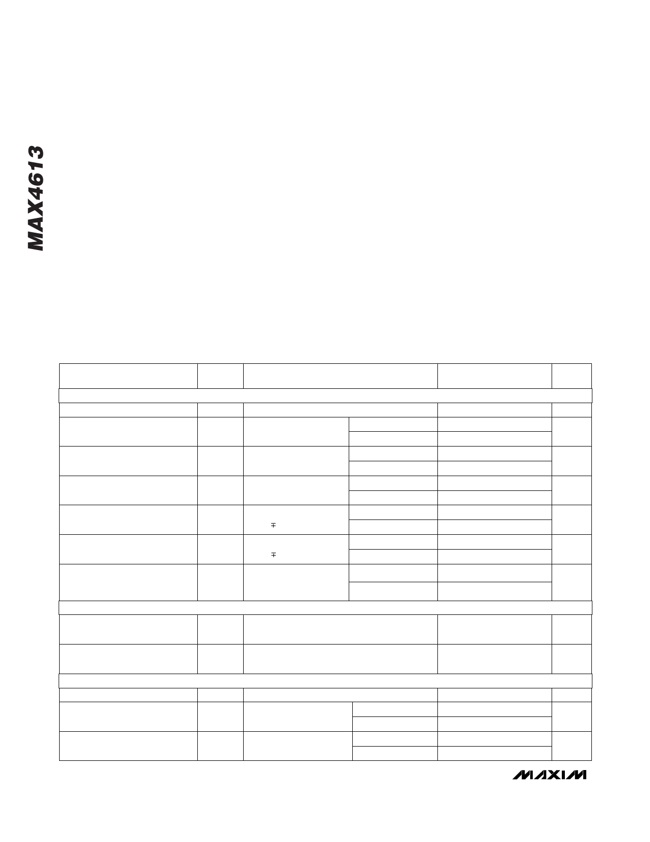
ELECTRICAL CHARACTERISTICS—Dual Supplies
(V+ = 15V, V- = -15V, VL = 5V, GND = 0V, VINH = 2.4V, VINL = 0.8V, TA = TMIN to TMAX, unless otherwise noted.)
PARAMETER
SYMBOL
CONDITIONS
SWITCH
Analog Signal Range
Drain-Source On-Resistance
VANALOG
RDS(ON)
(Note 3)
VD = ±10V,
IS = 1mA
On-Resistance Match
Between Channels (Note 4)
ΔRDS(ON)
VD = ±10V,
IS = 1mA
On-Resistance Flatness (Note 4) RFLAT(ON)
VD = ±5V,
IS = 1mA
Source Leakage Current
(Note 5)
IS(OFF)
VD = ±14V,
VS = 14V
Drain-Off Leakage Current
(Note 5)
Drain-On Leakage Current
(Note 5)
INPUT
ID(OFF)
ID(ON)
or
IS(ON)
VD = ±14V,
VS = 14V
VD = ±14V,
VS = ±14V
TA = +25°C
TA = TMIN to TMAX
TA = +25°C
TA = TMIN to TMAX
TA = +25°C
TA = TMIN to TMAX
TA = +25°C
TA = TMIN to TMAX
TA = +25°C
TA = TMIN to TMAX
TA = +25°C
TA = TMIN to TMAX
Input Current with
Input Voltage High
IINH VIN = 2.4V, all others = 0.8V
MIN TYP
(Note 2)
MAX
UNITS
-15
15
V
55
70
Ω
85
4
Ω
5
9
Ω
15
-0.50 0.01 0.50
nA
-5
5
-0.50 0.01 0.50
nA
-5
5
-0.50 0.08 0.50
nA
-10
10
-0.5 -0.00001 0.5
µA
Input Current with
Input Voltage Low
SUPPLY
Power-Supply Range
Positive Supply Current
Negative Supply Current
IINL VIN = 0.8V, all others = 2.4V
-0.5 -0.00001 0.5
µA
V+, V-
I+
I-
All channels on or off,
VIN = 0 or 5V
All channels on or off,
VIN = 0 or 5V
±4.5
±20.0
V
TA = +25°C
-1 0.001
1
µA
TA = TMIN to TMAX
-5
5
TA = +25°C
-1 0.001
1
µA
TA = TMIN to TMAX
-5
5
2 _______________________________________________________________________________________
Share Link: 