MAX5073 データシートの表示(PDF) - Maxim Integrated
部品番号
コンポーネント説明
メーカー
MAX5073 Datasheet PDF : 25 Pages
| |||
2.2MHz, Dual-Output Buck or Boost Converter
with Internal Power MOSFETs
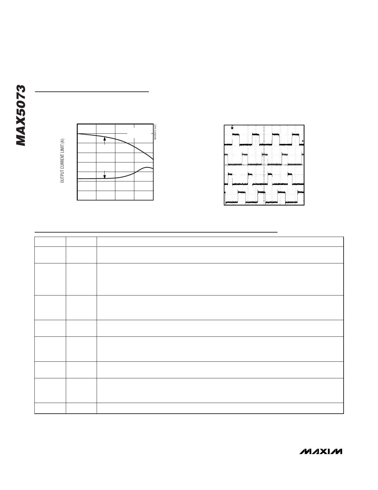
Typical Operating Characteristics (continued)
(V+ = VL = 5.2V, TA = +25°C, unless otherwise noted.)
OUTPUT LOAD CURRENT LIMIT
vs. TEMPERATURE
3.00
2.75
VIN = 5.5V
fSW = 2.2MHz
2.50
OUTPUT1
2.25
2.00
OUTPUT2
1.75
1.50
1.25
1.00
-40
-5
30
65
100
TEMPERATURE (°C)
FOUR-PHASE OPERATION
(SEE FIGURE 3)
MAX5073 toc22
SOURCE1
(MASTER)
0V
SOURCE2
(MASTER)
0V
SOURCE1
(SLAVE)
0V
400ns/div
SOURCE2
(SLAVE)
Pin Description
PIN
NAME
FUNCTION
1
CLKOUT Clock Output. CLKOUT is 45° phase-shifted with respect to converter 2 (SOURCE2, Figure 3). Connect
CLKOUT (master) to the SYNC of a second MAX5073 (slave) for a four-phase converter.
Buck Converter Operation—Bootstrap Flying-Capacitor Connection for Converter 2. Connect BST2/VDD2
2
BST2/VDD2
to an external ceramic capacitor and diode according to the standard application circuit (Figure 1).
Boost Converter Operation—Driver Bypass Capacitor Connection. Connect a low-ESR 0.1µF ceramic
capacitor from BST2/VDD2 to PGND (Figure 8).
Connection to Converter 2 Internal MOSFET Drain. Buck converter operation—use the MOSFET as a
3, 4
DRAIN2 high-side switch and connect DRAIN2 to the input supply. Boost converter operation—use the MOSFET
as a low-side switch and connect DRAIN2 to the inductor and diode junction (Figure 8).
5
EN2
Active-High Enable Input for Converter 2. Drive EN2 low to shut down converter 2, drive EN2 high for normal
operation. Use EN2 in conjunction with EN1 for supply sequencing. Connect to VL for always-on operation.
Feedback Input for Converter 2. Connect FB2 to a resistive divider between converter 2’s output and SGND
6
FB2 to adjust the output voltage. To set the output voltage below 0.8V, connect FB2 to a resistive voltage-divider
from BYPASS to regulator 2’s output (Figure 5). See the Setting the Output Voltage section.
7
COMP2
Compensation Connection for Converter 2. See the Compensation section to compensate converter 2’s
control loop.
External Clock Synchronization Input. Connect SYNC to a 400kHz to 4400kHz clock to synchronize the
8
SYNC switching frequency with the system clock. Each converter frequency is one half the frequency applied to
SYNC. Connect SYNC to SGND when not used.
9
N.C. No Connection. Not internally connected.
8 _______________________________________________________________________________________
Share Link: 