MAX5073 データシートの表示(PDF) - Maxim Integrated
部品番号
コンポーネント説明
メーカー
MAX5073 Datasheet PDF : 25 Pages
| |||
2.2MHz, Dual-Output Buck or Boost Converter
with Internal Power MOSFETs
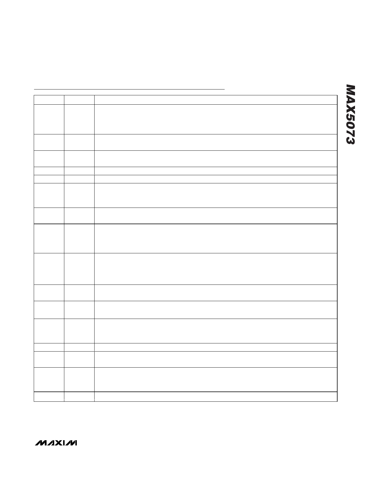
Pin Description (continued)
PIN
10
11
12, 13
14
15
16
17
18, 19
20
21
22
23, 24
25
26
27, 28
EP
NAME
OSC
V+
VL
BYPASS
COMP1
FB1
FUNCTION
Oscillator Frequency Set Input. Connect a resistor from OSC to SGND (ROSC) to set the switching
frequency (see the Oscillator section). Set ROSC for equal to or lower oscillator frequency than the SYNC
input frequency when using external synchronization (0.2fSYNC < fOSC < 1.2fSYNC). ROSC is still required
when an external clock is connected to the SYNC input.
Input Supply Voltage. V+ voltage range from 5.5V to 23V. Connect the V+ and VL together for 4.5V to
5.5V input operation. Bypass with a minimum 0.1µF ceramic capacitor to SGND.
Internal 5.2V Linear Regulator Output. Use VL to drive the high-side switch at BST1/VDD1 and
BST2/VDD2. Bypass VL with a 0.1µF capacitor to PGND and a 4.7µF ceramic capacitor to SGND.
2.0V Output. Bypass to SGND with a 0.22µF or greater ceramic capacitor.
Compensation Connection for Converter 1 (See the Compensation Section)
Feedback Input for Converter 1. Connect FB1 to a resistive divider between converter 1’s output and SGND
to program the output voltage. To set the output voltage below 0.8V, connect FB1 to a resistive voltage-
divider from BYPASS to regulator 1’s output (Figure 5). See the Setting the Output Voltage section.
EN1
DRAIN1
Active-High Enable Input for Converter 1. Drive EN1 low to shut down converter 1, drive EN1 high for normal
operation. Use EN1 in conjunction with EN2 for supply sequencing. Connect to VL for always-on operation.
Connection to the Converter 1 Internal MOSFET Drain.
Buck converter operation—use the MOSFET as a high-side switch and connect DRAIN1 to the input supply.
Boost converter operation—use the MOSFET as a low-side switch and connect DRAIN1 to the inductor
and diode junction.
Buck Converter Operation—Bootstrap Flying-Capacitor Connection for Converter 1. Connect BST1/VDD1
BST1/VDD1
to an external ceramic capacitor and diode according to the Standard Application Circuit (Figure 1).
Boost Converter Operation—Driver Bypass Capacitor Connection. Connect a low-ESR 0.1µF ceramic
capacitor from BST1/VDD1 to PGND.
PGOOD1
Converter 1 Power-Good Output. Open-drain output goes low when converter 1’s output falls below
92.5% of its set regulation voltage. Use PGOOD1, PGOOD2, EN1, and EN2 to sequence the converters.
PGOOD2
Converter 2 Power-Good Output. Open-drain output goes low when converter 2’s output falls below
92.5% of its set regulation voltage.
Connection to the Converter 1 Internal MOSFET Source.
SOURCE1 Buck converter operation—connect SOURCE1 to the switched side of the inductor as shown in Figure 1.
Boost converter operation—connect SOURCE1 to PGND.
SGND
PGND
Signal Ground. Connect SGND to the exposed pad. Connect SGND and PGND together at a single point.
Power Ground. Connect rectifier diode anode, input capacitor negative, output capacitor negative, and
VL bypass capacitor returns to PGND.
Connection to the Converter 2 Internal MOSFET Source.
SOURCE2 Buck converter operation—connect SOURCE2 to the switched side of the inductor as shown in Figure 1.
Boost converter operation—connect SOURCE2 to PGND (Figure 8).
SGND Exposed Paddle. Connect to SGND. Solder EP to the SGND plane for better thermal performance.
_______________________________________________________________________________________ 9
Share Link: 