MAX6877 データシートの表示(PDF) - Maxim Integrated
部品番号
コンポーネント説明
メーカー
MAX6877 Datasheet PDF : 24 Pages
| |||
Dual-/Triple-Voltage, Power-Supply
Trackers/Sequencers/Supervisors
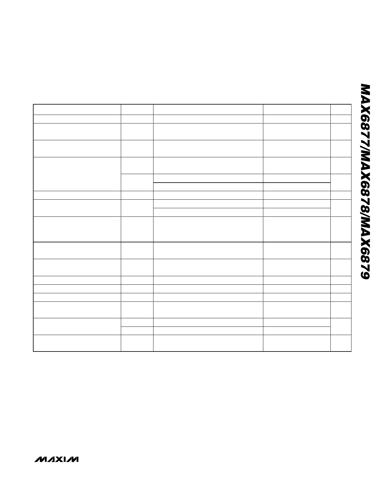
ELECTRICAL CHARACTERISTICS (continued)
(VCC, IN1, IN2, or IN3 = +2.7V to +5.5V, EN/UV = MARGIN = ABP, TA = -40°C to +85°C, unless otherwise specified. Typical values
are at TA = +25°C, unless otherwise noted.) (Note 1)
PARAMETER
SYMBOL
CONDITIONS
Power-Good Threshold Hysteresis VHYS_PG VOUT_ rising
GATE_ Output High
VGOH ISOURCE = 0.5µA
GATE_ Pullup Current
GATE_ Pulldown Current
SET_ to GATE_ Delay
FAULT, PG/RST Output Low
Tracking Differential Voltage Stop
Ramp
IGUP
IGD
IGDS
tD-GATE
VOL
VTRK
During power-up and power-down,
VGATE_ = 1V
During power-up and power-down,
VGATE_ = 5V
When disabled, VGATE_ = 5V, VIN_ ≥ 2.7V
When disabled, VGATE_ = 5V, VIN_ ≥ 4V
SET falling, 25mV overdrive
VIN_ ≥ 2.7V, ISINK = 1mA, output asserted
VIN_ ≥ 4.0V, ISINK = 4mA, output asserted
Differential between each of the OUT_ and
the ramp voltage during power-up and
power-down, Figure 10 (Note 5)
MIN
IN_ +
4.2
TYP
0.5
IN_ +
5.0
MAX
IN_ +
5.8
UNITS
%
V
2.5
4
µA
2.5
4
µA
9.5
mA
20
6
µs
0.3
V
0.4
75
125
180
mV
Tracking Differential Fault Voltage
VTRK_F
Differential between each of the OUT_ and
the ramp voltage, Figure 10 (Note 5)
200
250
310
mV
Tracking Differential Voltage
Hysteresis
Power-Low Threshold
Power-Low Hysteresis
OUT to GND Pulldown Impedance
MARGIN, TRK/SEQ, LTCH/RTR
Pullup Current
MARGIN, TRK/SEQ, LTCH/RTR
Input Voltage
MARGIN, TRK/SEQ, LTCH/RTR
Glitch Rejection
VTH_PL
VTH_PLHYS
IIN
VIL
VIH
OUT_ falling
OUT_ rising
VABP > 2.7V (Note 6)
20
%
125
142
170
mV
10
mV
100
Ω
7
10
13
µA
0.8
V
2.0
100
ns
Note 1: Specifications guaranteed for the stated global conditions. 100% production tested at TA = +25°C and TA = +85°C.
Specifications at TA = -40°C to +85°C are guaranteed by design. These devices meet the parameters specified when at
least one of VCC, IN1/IN2/IN3 is between 2.7V to 5.5V, while the remaining IN1/IN2/IN3 are between 0 and 5.5V.
Note 2: A current ID = 2.5µA ±15% is generated internally and is used to set the DELAY and TIMEOUT periods and used as a refer-
ence for tDELAY and tTIMEOUT.
Note 3: The total DELAY is tDELAY = 200ms + (500kΩ x CDELAY). Leave DELAY unconnected for 200µs delay. The total TIMEOUT is
tTIMEOUT = 200µs + (500kΩ x CTIMEOUT). Leave TIMEOUT unconnected for 200µs timeout.
Note 4: A current IS = 25µA ±10% is generated internally and used as a reference for tFAULT, tRETRY, and slew rate.
Note 5: During power-up, only the condition OUT_ < ramp - VTRK is checked in order to stop the ramp. However, both conditions
OUT_ < ramp - VTRK_F and OUT_ > ramp + VTRK_F cause a fault. During power-down, only the condition OUT > ramp +
VTRK is checked in order to stop the ramp. However, both conditions OUT_ < ramp - VTRK_F and OUT_ > ramp + VTRK_F
cause a fault (see Figure 10). Therefore, if OUT1, OUT2, and OUT3 (during power-up tracking and power-down) differ by
more than 2 x VTRK_F, a fault condition is asserted.
Note 6: A 100Ω pulldown to GND activated by a fault condition. See the Internal Pulldown section.
_______________________________________________________________________________________ 3
Share Link: 