MAX6880 データシートの表示(PDF) - Maxim Integrated
部品番号
コンポーネント説明
メーカー
MAX6880 Datasheet PDF : 19 Pages
| |||
Dual-/Triple-Voltage, Power-Supply
Sequencers/Supervisors
ABSOLUTE MAXIMUM RATINGS
(All voltages referenced to GND, unless otherwise noted.)
IN1, IN2, IN3.............................................................-0.3V to +6V
ABP .........................................-0.3V to the highest of VIN1 - VIN3
SET1, SET2, SET3 ....................................................-0.3V to +6V
GATE1, GATE2, GATE3 .........................................-0.3V to +12V
OUT1, OUT2, OUT3 .................................................-0.3V to +6V
MARGIN ...................................................................-0.3V to +6V
PG/RST, EN/UV ........................................................-0.3V to +6V
DELAY, SLEW, TIMEOUT .........................................-0.3V to +6V
OUT_ Current....................................................................±50mA
GND Current.....................................................................±50mA
Input/Output Current (all pins except
OUT_ and GND) ...........................................................±20mA
Continuous Power Dissipation (TA = +70°C)
16-Pin 4mm x 4mm Thin QFN
(derate 16.9mW/°C above +70°C) .............................1349mW
24-Pin 4mm x 4mm Thin QFN
(derate 20.8mW/°C above +70°C) .............................1667mW
Operating Temperature Range ...........................-40°C to +85°C
Storage Temperature Range .............................-65°C to +150°C
Maximum Junction Temperature .....................................+150°C
Lead Temperature (soldering, 10s) .................................+300°C
Stresses beyond those listed under “Absolute Maximum Ratings” may cause permanent damage to the device. These are stress ratings only, and functional
operation of the device at these or any other conditions beyond those indicated in the operational sections of the specifications is not implied. Exposure to
absolute maximum rating conditions for extended periods may affect device reliability.
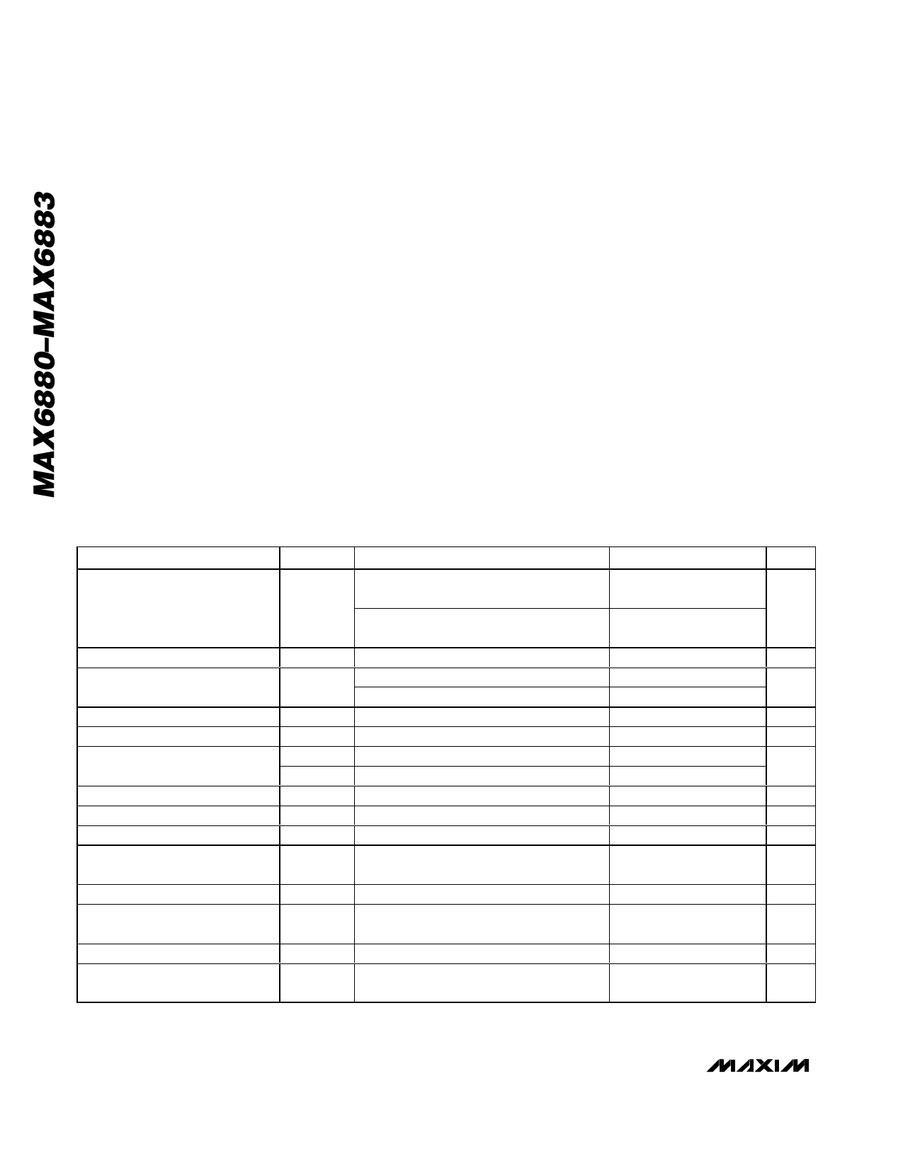
ELECTRICAL CHARACTERISTICS
(IN1, IN2, or IN3 = +2.7V to +5.5V, EN/UV = MARGIN = ABP, TA = -40°C to +85°C, unless otherwise specified. Typical values are
at TA = +25°C, unless otherwise noted.) (Note 1)
PARAMETER
Operating Voltage Range
Supply Current
SET_ Threshold Range
SET_ Threshold Hysteresis
SET_ Input Current
EN/UV Input Voltage
EN/UV Input Current
EN/UV Input Pulse Width
DELAY, TIMEOUT Output Current
DELAY, TIMEOUT Threshold
Voltage
SLEW Output Current
Sequence Slew-Rate Timebase
Accuracy
Timebase/CSLEW Ratio
Slew-Rate Accuracy during Power-
Up and Power-Down
SYMBOL
IN_
ICC
VTH
VTH_HYST
ISET
VEN_R
VEN_F
IEN
tEN
ID
CONDITIONS
Voltage on the highest of IN_ to ensure that
PG/RST is valid and GATE_ = 0
Voltage on the highest of IN_ to ensure the
device is fully operational
IN1 = 5.5V, IN2 = IN3 = 3.3V, no load
SET_ falling, TA = +25oC
SET_ falling, TA = -40 °C to +85°C
SET_ rising
SET_ = 0.5V
Input rising
Input falling
EN/UV falling, 100mV overdrive
(Notes 2, 3)
VCC = 3.3V
IS
(Note 4)
SR
CSLEW = 200pF
100pF < CSLEW < 1nF
CSLEW = 200pF, VIN_ = 5.5V (Note 4)
MIN TYP MAX UNITS
1.4
V
2.7
5.5
1.1
1.8
mA
0.4925 0.5 0.5075
V
0.4875 0.5 0.5125
0.5
%
-100
+100 nA
1.286
V
1.22 1.25 1.28
-5
+5
µA
7
µs
2.12
2.5
2.88
µA
1.25
V
22.5
25
27.5
µA
-15
+15
%
104
kΩ
-50
+50
%
2 _______________________________________________________________________________________
Share Link: 