MAX7031 データシートの表示(PDF) - Maxim Integrated
部品番号
コンポーネント説明
メーカー
MAX7031
Maxim Integrated

MAX7031 Datasheet PDF : 20 Pages
| |||
Low-Cost, 308MHz, 315MHz, and 433.92MHz
FSK Transceiver with Fractional-N PLL
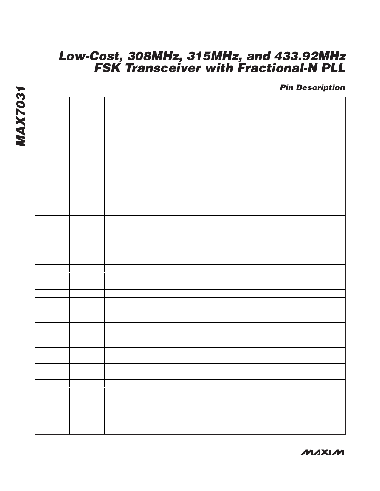
Pin Description
PIN
NAME
FUNCTION
1
PAVDD
Power-Amplifier Supply Voltage. Bypass to GND with 0.01µF and 220pF capacitors placed as close
as possible to the pin.
Envelope-Shaping Output. ROUT controls the power-amplifier envelope’s rise and fall times. Connect
ROUT to the PA pullup inductor or optional power-adjust resistor. Bypass the inductor to GND as
2
ROUT
close as possible to the inductor with 680pF and 220pF capacitors as shown in the Typical
Application Circuit.
3
TX/RX1 Transmit/Receive Switch Throw. Drive T/R high to short TX/RX1 to TX/RX2. Drive T/R low to disconnect
TX/RX1 from TX/RX2. Functionally identical to TX/RX2.
4
TX/RX2 Transmit/Receive Switch Pole. Typically connected to ground. See the Typical Application Circuit.
5
PAOUT
Power-Amplifier Output. Requires a pullup inductor to the supply voltage (or ROUT if envelope
shaping is desired), which can be part of the output-matching network to an antenna.
6
AVDD
Analog Power-Supply Voltage. AVDD is connected to an on-chip +3.0V regulator in 5V operation.
Bypass AVDD to GND with a 0.1µF and 220pF capacitor placed as close as possible to the pin.
7
LNAIN Low-Noise Amplifier Input. Must be AC-coupled.
8
LNASRC
Low-Noise Amplifier Source for External Inductive Degeneration. Connect an inductor to GND to set
the LNA input impedance.
9
LNAOUT
Low-Noise Amplifier Output. Must be connected to AVDD through a parallel LC tank filter. AC-couple
to MIXIN+.
10
MIXIN+ Noninverting Mixer Input. Must be AC-coupled to the LNA output.
11
MIXIN- Inverting Mixer Input. Bypass to AVDD with a capacitor as close as possible to the LNA LC tank filter.
12
MIXOUT 330Ω Mixer Output. Connect to the input of the 10.7MHz filter.
13
IFIN-
Inverting 330Ω IF Limiter Amplifier Input. Bypass to GND with a capacitor.
14
IFIN+
Noninverting 330Ω IF Limiter Amplifier Input. Connect to the output of the 10.7MHz IF filter.
15
PDMIN Minimum-Level Peak Detector for Demodulator Output
16
PDMAX Maximum-Level Peak Detector for Demodulator Output
17
DS-
Inverting Data Slicer Input
18
DS+
Noninverting Data Slicer Input
19
OP+
Noninverting Op-Amp Input for the Sallen-Key Data Filter
20
DF
Data-Filter Feedback Node. Input for the feedback capacitor of the Sallen-Key data filter.
21
RSSI
Buffered Received-Signal-Strength-Indicator Output
22
T/R
Transmit/Receive. Drive high to put the device in transmit mode. Drive low or leave unconnected to
put the device in receive mode. It is internally pulled down.
23
ENABLE
Enable. Drive high for normal operation. Drive low or leave unconnected to put the device into
shutdown mode.
24
DATA Receiver Data Output/Transmitter Data Input
25
N.C.
No Connection. Do not connect to this pin.
26
DVDD
Digital Power-Supply Voltage. Bypass to GND with a 0.01µF and 220pF capacitor placed as close as
possible to the pin.
High-Voltage Supply Input. For 3V operation, connect HVIN to AVDD, PAVDD, and DVDD. For 5V
27
HVIN
operation, connect only HVIN to 5V. Bypass HVIN to GND with a 0.01µF and 220pF capacitor placed
as close as possible to the pin.
10 ______________________________________________________________________________________
Share Link: