MAX7034 データシートの表示(PDF) - Maxim Integrated
部品番号
コンポーネント説明
メーカー
MAX7034 Datasheet PDF : 14 Pages
| |||
MAX7034
315MHz/434MHz ASK Superheterodyne
Receiver
Absolute Maximum Ratings
VDD5 to AGND......................................................-0.3V to +6.0V
AVDD to AGND.....................................................-0.3V to +4.0V
DVDD to DGND.....................................................-0.3V to +4.0V
AGND to DGND....................................................-0.1V to +0.1V
IRSEL, DATAOUT, XTALSEL,
SHDN, EN_REG to AGND.................. -0.3V to (VDD5 + 0.3V)
All Other Pins to AGND.........................-0.3V to (VDVDD + 0.3V)
Continuous Power Dissipation (TA = +70°C)
28-Pin TSSOP (derate 12.8mW/°C above +70°C)...1025.6mW
Operating Temperature Range.......................... -40°C to +125°C
Storage Temperature Range............................. -65°C to +150°C
Junction Temperature.......................................................+150°C
Lead Temperature (soldering, 10s).................................. +300°C
Soldering Temperature (reflow)........................................+260°C
Stresses beyond those listed under “Absolute Maximum Ratings” may cause permanent damage to the device. These are stress ratings only, and functional operation of the device at these
or any other conditions beyond those indicated in the operational sections of the specifications is not implied. Exposure to absolute maximum rating conditions for extended periods may affect
device reliability.
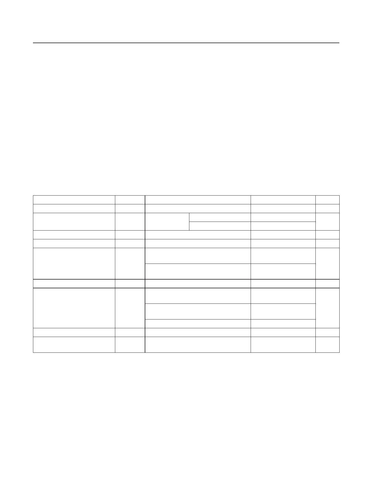
DC Electrical Characteristics
(Typical Application Circuit, VDD5 = +4.5V to +5.5V, no RF signal applied. TA = -40°C to +125°C, unless otherwise noted. Typical values
are at VDD5 = +5.0V and TA = +25°C, unless otherwise noted.) (Note 1)
PARAMETER
Supply Voltage
Supply Current
Shutdown Supply Current
Input-Voltage Low
Input-Voltage High
Input Logic Current High
Image-Reject Select Voltage
(Note 2)
DATAOUT Voltage-Output Low
DATAOUT Voltage-Output High
SYMBOL
VDD5
IDD
ISHDN
VIL
CONDITIONS
+5.0V nominal supply voltage
VSHDN = VDD5
VSHDN = 0V
fRF = 315MHz
fRF = 433MHz
EN_REG, SHDN
VIH
XTALSEL
IIH
fRF = 433MHz, VIRSEL = VDVDD
VOL
VOH
fRF = 375MHz, VIRSEL = VDVDD/2
fRF = 315MHz, VIRSEL = 0V
ISINK = 10µA
ISOURCE = 10µA
MIN
4.5
VDD5 -
0.4
VDVDD
- 0.4
VDVDD
- 0.4
1.1
TYP
5.0
6.7
7.2
3
15
0.125
VDD5 -
0.125
MAX
5.5
8.2
8.7
8
0.4
VDVDD
- 1.5
0.4
UNITS
V
mA
µA
V
V
µA
V
V
V
www.maximintegrated.com
Maxim Integrated │ 2
Share Link: 