M50LPW116 データシートの表示(PDF) - STMicroelectronics
部品番号
コンポーネント説明
メーカー
M50LPW116 Datasheet PDF : 36 Pages
| |||
M50LPW116
8KBytes, 1 Main Block of 32KBytes, 30 Main
Blocks of 64KBytes and 16 Parameter Blocks of
4KBytes.
Two different bus interfaces are supported by the
memory. The primary interface is the Low Pin
Count (or LPC) Standard Interface. This has been
designed to remove the need for the ISA bus in
current PC Chipsets; the M50LPW116 acts as the
PC BIOS on the Low Pin Count bus for these PC
Chipsets.
The secondary interface, the Address/Address
Multiplexed (or A/A Mux) Interface, is designed to
be compatible with current Flash Programmers for
production line programming prior to fitting to a PC
Motherboard.
The memory is offered in TSOP40 (10 x 20mm)
package and it is supplied with all the bits erased
(set to ’1’).
SIGNAL DESCRIPTIONS
There are two different bus interfaces available on
this part. The active interface is selected before
power-up or during Reset using the Interface Con-
figuration Pin, IC.
The signals for each interface are discussed in the
Low Pin Count (LPC) Signal Descriptions section
and the Address/Address Multiplexed (A/A Mux)
Signal Descriptions section below. The supply sig-
nals are discussed in the Supply Signal Descrip-
tions section below.
Low Pin Count (LPC) Signal Descriptions
For the Low Pin Count (LPC) Interface see Figure
1, Logic Diagram (LPC Interface), and Table 1,
Signal Names (LPC Interface).
The LPC address sequence is 32 bits long. The
M50LPW116 responds to addresses mapped to
the top of the 4 GByte memory space, from
FFFF FFFFh. Address bits A31-A26 must be set
to 1. For A25-A23 and A21, refer to Table 2. A22
is set to 1 for array access, and to 0 for register ac-
cess. A20-A0 are for array addresses.
Input/Output Communications (LAD0-LAD3). All
Input and Output Communication with the memory
take place on these pins. Addresses and Data for
Bus Read and Bus Write operations are encoded
on these pins.
Input Communication Frame (LFRAME). The
Input Communication Frame (LFRAME) signals
the start of a bus operation. When Input Commu-
nication Frame is Low, VIL, on the rising edge of
the Clock a new bus operation is initiated. If Input
Communication Frame is Low, VIL, during a bus
operation then the operation is aborted. When In-
put Communication Frame is High, VIH, the cur-
rent bus operation is proceeding or the bus is idle.
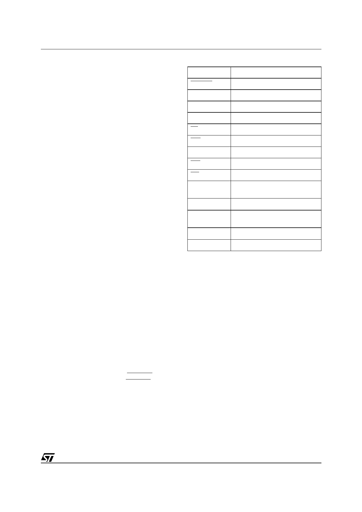
Table 1. Signal Names (LPC Interface)
LAD0-LAD3
Input/Output Communications
LFRAME
Input Communication Frame
ID0-ID3
Identification Inputs
GPI0-GPI4
General Purpose Inputs
IC
Interface Configuration
RP
Interface Reset
INIT
CPU Reset
CLK
Clock
TBL
Top Block Lock
WP
Write Protect
RFU
Reserved for Future Use. Leave
disconnected.
VCC
Supply Voltage
VPP
Optional Supply Voltage for Fast
Program and Fast Erase Operations
VSS
Ground
NC
Not Connected Internally
Identification Inputs (ID0-ID3). The Identification
Inputs (ID0-ID3) allow to address up to 16
memories on a bus. The value on addresses
A21,A23-A25 is compared to the hardware
strapping on the ID0-ID3 pins to select which
memory is being addressed. For an address bit to
be ‘1’ the correspondent ID pin can be left floating
or driven Low, VIL; an internal pull-down resistor is
included with a value of RIL. For an address bit to
be ‘0’ the correspondent ID pin must be driven
High, VIH; there will be a leakage current of ILI2
through each pin when pulled to VIH; see Table 20.
By convention the boot memory must have ID0-
ID3 pins left floating or driven Low, VIL and a ‘1’
value on A21,A23-A25 and all additional
memories take sequential ID0-ID3 configuration,
as shown in Table 2.
General Purpose Inputs (GPI0-GPI4). The Gener-
al Purpose Inputs can be used as digital inputs for
the CPU to read. The General Purpose Input Reg-
ister holds the values on these pins. The pins must
have stable data from before the start of the cycle
that reads the General Purpose Input Register un-
til after the cycle is complete. These pins must not
be left to float, they should be driven Low, VIL, or
High, VIH.
3/36
Share Link: 