M50LPW116 データシートの表示(PDF) - STMicroelectronics
部品番号
コンポーネント説明
メーカー
M50LPW116 Datasheet PDF : 36 Pages
| |||
M50LPW116
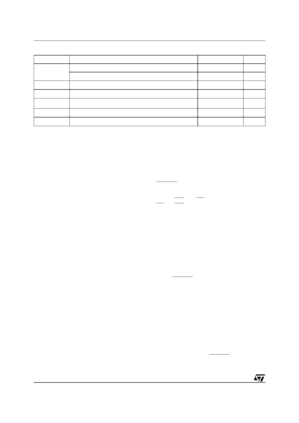
Table 4. Absolute Maximum Ratings (1)
Symbol
Parameter
Value
Unit
Ambient Operating Temperature (Temperature Range Option 1)
0 to 70
°C
TA
Ambient Operating Temperature (Temperature Range Option 5)
–20 to 85
°C
TBIAS
Temperature Under Bias
–50 to 125
°C
TSTG
Storage Temperature
–65 to 150
°C
VIO (2)
Input or Output Voltage
–0.6 to VCC + 0.6
V
VCC
Supply Voltage
–0.6 to 4
V
VPP
Program Voltage
–0.6 to 13
V
Note: 1. Except for the rating "Operating Temperature Range", stresses above those listed in the Table "Absolute Maximum Ratings" may
cause permanent damage to the device. These are stress ratings only and operation of the device at these or any other conditions
above those indicated in the Operating sections of this specification is not implied. Exposure to Absolute Maximum Rating condi-
tions for extended periods may affect device reliability. Refer also to the STMicroelectronics SURE Program and other relevant qual-
ity documents.
2. Minimum Voltage may undershoot to –2V and for less than 20ns during transitions. Maximum Voltage may overshoot to VCC +2V
and for less than 20ns during transitions.
VPP Optional Supply Voltage. The VPP Optional
Supply Voltage pin is used to select the Fast
Program (see the Quadruple Byte Program
Command description) and Fast Erase options of
the memory and to protect the memory. When
VPP < VPPLK Program and Erase operations
cannot be performed and an error is reported in
the Status Register if an attempt to change the
memory contents is made. When VPP = VCC
Program and Erase operations take place as
normal. When VPP = VPPH Fast Program
operations (using the Quadruple Byte Program
command, 30h, from Table 11) and Fast Erase
operations are used. Any other voltage input to
VPP will result in undefined behavior and should
not be used.
VPP should not be set to VPPH for more than 80
hours during the life of the memory.
VSS Ground. VSS is the reference for all the volt-
age measurements.
BUS OPERATIONS
The two interfaces have similar bus operations but
the signals and timings are completely different.
The Low Pin Count (LPC) Interface is the usual
interface and all of the functionality of the part is
available through this interface. Only a subset of
functions are available through the Address/
Address Multiplexed (A/A Mux) Interface.
Follow the section Low Pin Count (LPC) Bus
Operations below and the section Address/
Address Multiplexed (A/A Mux) Interface Bus
Operations below for a description of the bus
operations on each interface.
Low Pin Count (LPC) Bus Operations
The Low Pin Count (LPC) Interface consists of
four data signals (LAD0-LAD3), one control line
(LFRAME) and a clock (CLK). In addition
protection against accidental or malicious data
corruption can be achieved using two further
signals (TBL and WP). Finally two reset signals
(RP and INIT) are available to put the memory into
a known state.
The data signals, control signal and clock are
designed to be compatible with PCI electrical
specifications. The interface operates with clock
speeds up to 33MHz.
The following operations can be performed using
the appropriate bus cycles: Bus Read, Bus Write,
Standby, Reset and Block Protection.
Bus Read. Bus Read operations read from the
memory cells, specific registers in the Command
Interface or Low Pin Count Registers. A valid Bus
Read operation starts when Input Communication
Frame, LFRAME, is Low, VIL, as Clock rises and
the correct Start cycle is on LAD0-LAD3. On the
following clock cycles the Host will send the Cycle
Type + Dir, Address and other control bits on
LAD0-LAD3. The memory responds by outputting
Sync data until the wait-states have elapsed
followed by Data0-Data3 and Data4-Data7.
See Table 6, and to Figure 4, for a description of
the Field definitions for each clock cycle of the
transfer. See Table 22, and Figure 9, for details on
the timings of the signals.
Bus Write. Bus Write operations write to the
Command Interface or Low Pin Count Registers. A
valid Bus Write operation starts when Input
Communication Frame, LFRAME, is Low, VIL, as
Clock rises and the correct Start cycle is on LAD0-
6/36
Share Link: 