M50LPW116 データシートの表示(PDF) - STMicroelectronics
部品番号
コンポーネント説明
メーカー
M50LPW116 Datasheet PDF : 36 Pages
| |||
M50LPW116
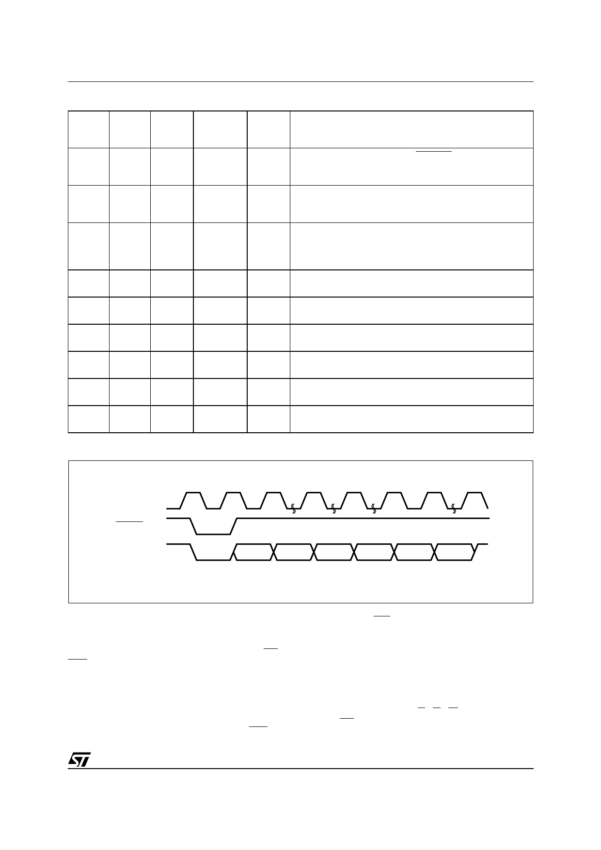
Table 7. LPC Bus Write Field Definitions
Clock Clock
Cycle Cycle
Number Count
Field
LAD0-
LAD3
Memory
I/O
Description
On the rising edge of CLK with LFRAME Low, the contents
1
1
START 0000b
I
of LAD0-LAD3 must be 0000b to indicate the start of a LPC
cycle.
CYCTY
Indicates the type of cycle. Bits 3:2 must be 01b. Bit 1
2
1
PE +
011Xb
I
indicates the direction of transfer: 1b for write. Bit 0 is don’t
DIR
care (X).
3-10
8
ADDR
XXXX
A 32-bit address phase is transferred starting with the most
I
significant nibble first. A26-A31 must be set to 1. A22 = 1 for
Array, A22 = 0 for registers access. For A21, A23-A25
values, refers to Table 2.
11-12
2
DATA
XXXX
I
Data transfer is two cycles, starting with the least significant
nibble.
13
1
TAR
1111b
I
The host drives LAD0-LAD3 to 1111b to indicate a
turnaround cycle.
14
1
TAR
1111b
(float)
O
The LPC Flash Memory takes control of LAD0-LAD3 during
this cycle.
15
1
SYNC
0000b
O
The LPC Flash Memory drives LAD0-LAD3 to 0000b,
indicating it has received data or a command.
16
1
TAR
1111b
O
The LPC Flash Memory drives LAD0-LAD3 to 1111b,
indicating a turnaround cycle.
17
1
TAR
1111b
(float)
N/A
The LPC Flash Memory floats its outputs and the host takes
control of LAD0-LAD3.
Figure 5. LPC Bus Write Waveforms
CLK
LFRAME
LAD0-LAD3
Number of
clock cycles
START
1
CYCTYPE
+ DIR
1
ADDR
8
DATA
2
TAR
2
SYNC
1
TAR
2
AI04430
Low, VIL, for tPLPH. The memory resets to Read
mode upon return from Reset mode and the Lock
Registers return to their default states regardless
of their state before Reset, see Table 15. If RP or
INIT goes Low, VIL, during a Program or Erase
operation, the operation is aborted and the
memory cells affected no longer contain valid
data; the memory can take up to tPLRH to abort a
Program or Erase operation.
Block Protection. Block Protection can be
forced using the signals Top Block Lock, TBL, and
Write Protect, WP, regardless of the state of the
Lock Registers.
Address/Address Multiplexed (A/A Mux) Bus
Operations
The Address/Address Multiplexed (A/A Mux)
Interface has a more traditional style interface.
The signals consist of a multiplexed address
signals (A0-A10), data signals, (DQ0-DQ7) and
three control signals (RC, G, W). An additional
signal, RP, can be used to reset the memory.
9/36
Share Link: 