M50FW016 データシートの表示(PDF) - STMicroelectronics
部品番号
コンポーネント説明
メーカー
M50FW016 Datasheet PDF : 45 Pages
| |||
M50FW016
Table 4. FWH Bus Read Field Definitions
Clock Clock
Cycle Cycle
Number Count
Field
FWH0- Memory
FWH3
I/O
Description
1
1
START 1101b
I
On the rising edge of CLK with FWH4 Low, the contents of
FWH0-FWH3 indicate the start of a FWH Read cycle.
Indicates which FWH Flash Memory is selected. The value
2
1
IDSEL
XXXX
I
on FWH0-FWH3 is compared to the IDSEL strapping on the
FWH Flash Memory pins to select which FWH Flash
Memory is being addressed.
3-9
7
ADDR
XXXX
A 28-bit address phase is transferred starting with the most
significant nibble first. For the multi-byte read operation, the
I
least significant bits (MSIZE of them) are treated as Don't
Care, and the read operation is started with each of these
bits reset to 0.
This one clock cycle is driven by the host to determine how
10
1
MSIZE 0XXXb
I
many bytes will be transferred. M50FW016 will support:
single byte transfer (0000b), 4-byte transfer (0010b), 16-byte
transfer (0100b) and 128-byte transfer (0111b).
11
1
TAR
1111b
I
The host drives FWH0-FWH3 to 1111b to indicate a
turnaround cycle.
12
1
TAR
1111b
(float)
O
The FWH Flash Memory takes control of FWH0-FWH3
during this cycle.
13-14
2
WSYNC 0101b
The FWH Flash Memory drives FWH0-FWH3 to 0101b
O (short wait-sync) for two clock cycles, indicating that the data
is not yet available. Two wait-states are always included.
The FWH Flash Memory drives FWH0-FWH3 to 0000b,
15
1
RSYNC 0000b
O indicating that data will be available during the next clock
cycle.
16-17
2
DATA
XXXX
Data transfer is two CLK cycles, starting with the least
O significant nibble. If multi-byte read operation is
enabled, repeat cycle 16-17 n times, where n = 2MSIZE – 1
Note 1
1
TAR
1111b
O
The FWH Flash Memory drives FWH0-FWH3 to 1111b to
indicate a turnaround cycle.
Note 2
1
TAR
1111b
(float)
N/A
Note: 1. Clock Cycle Number = (2MSIZE – 1) * 2 + 18
2. Clock Cycle Number = (2MSIZE – 1) * 2 + 19
The FWH Flash Memory floats its outputs, the host takes
control of FWH0-FWH3.
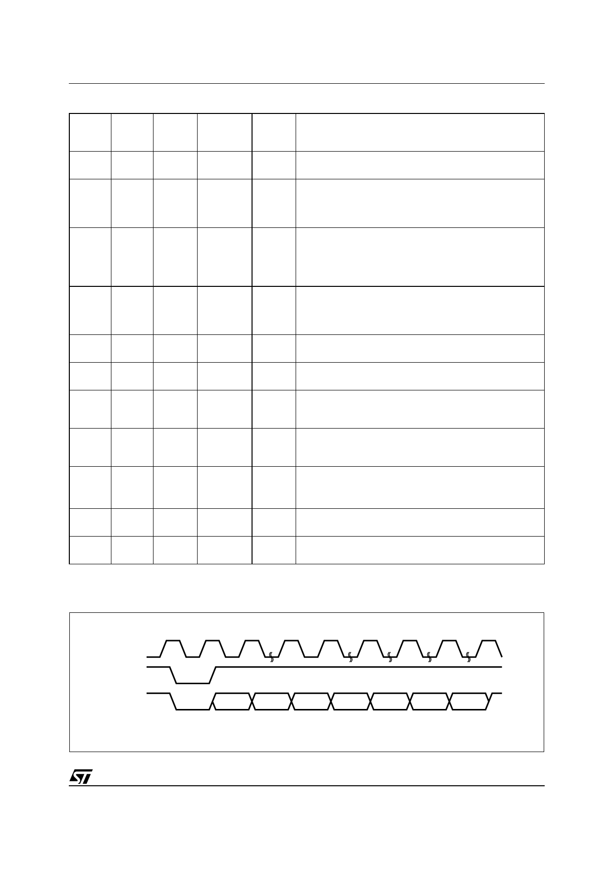
Figure 5. FWH Bus Read Waveforms (Single Byte Read)
CLK
FWH4
FWH0-FWH3
Number of
clock cycles
START
1
IDSEL
1
ADDR
7
MSIZE
1
TAR
2
SYNC
3
DATA
2
TAR
2
AI03437
13/45
Share Link: 