M50FW016 データシートの表示(PDF) - STMicroelectronics
部品番号
コンポーネント説明
メーカー
M50FW016 Datasheet PDF : 45 Pages
| |||
M50FW016
Table 6. FWH Bus Write Field Definitions (Quadruple Byte Program)
Clock Clock
Cycle Cycle
Number Count
Field
FWH0- Memory
FWH3
I/O
Description
1
1
START
1110b
I
On the rising edge of CLK with FWH4 Low, the contents of
FWH0-FWH3 indicate the start of a FWH Write Cycle.
Indicates which FWH Flash Memory is selected. The value
2
1
IDSEL
XXXX
I
on FWH0-FWH3 is compared to the IDSEL strapping on the
FWH Flash Memory pins to select which FWH Flash
Memory is being addressed.
3-9
7
ADDR
XXXX
A 28-bit address phase is transferred starting with the most
I
significant nibble first. The A1-A0 lines are treated as Don't
Care.
10
1
MSIZE 0010b
I
Always 0010b (quadruple byte transfer).
11-18
8
DATA
XXXX
Data transfer is two cycles, starting with the least significant
nibble. (The first pair of nibbles is that at the address with A1-
I
A0 set to 00, the second pair with A1-A0 set to 01, the third
pair with A1-A0 set to 10, and the fourth pair with A1-A0 set
to 11.)
19
1
TAR
1111b
I
The host drives FWH0-FWH3 to 1111b to indicate a
turnaround cycle.
20
1
TAR
1111b
(float)
O
The FWH Flash Memory takes control of FWH0-FWH3
during this cycle.
21
1
SYNC
0000b
O
The FWH Flash Memory drives FWH0-FWH3 to 0000b,
indicating it has received data or a command.
22
1
TAR
1111b
O
The FWH Flash Memory drives FWH0-FWH3 to 1111b,
indicating a turnaround cycle.
23
1
TAR
1111b
(float)
N/A
The FWH Flash Memory floats its outputs and the host takes
control of FWH0-FWH3.
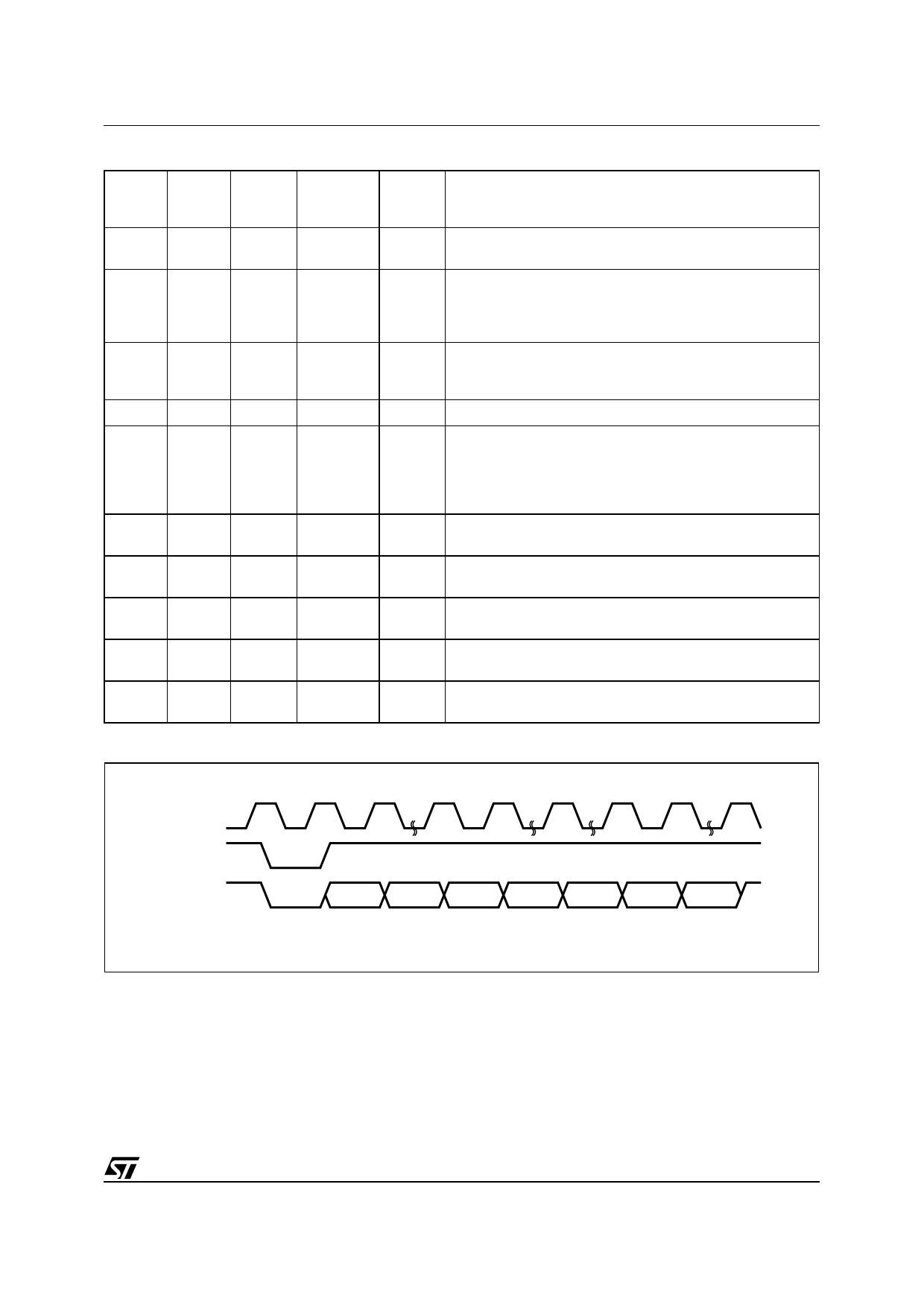
Figure 7. FWH Bus Write Waveforms (Quadruple Byte Program)
CLK
FWH4
FWH0-FWH3
Number of
clock cycles
START
1
IDSEL
1
ADDR
7
MSIZE
1
DATA
8
TAR
2
SYNC
1
TAR
2
AI05784
15/45
Share Link: 