MAX924CSE データシートの表示(PDF) - Maxim Integrated
部品番号
コンポーネント説明
メーカー
MAX924CSE Datasheet PDF : 17 Pages
| |||
Ultra Low-Power,
Single/Dual-Supply Comparators
_______________Detailed Description
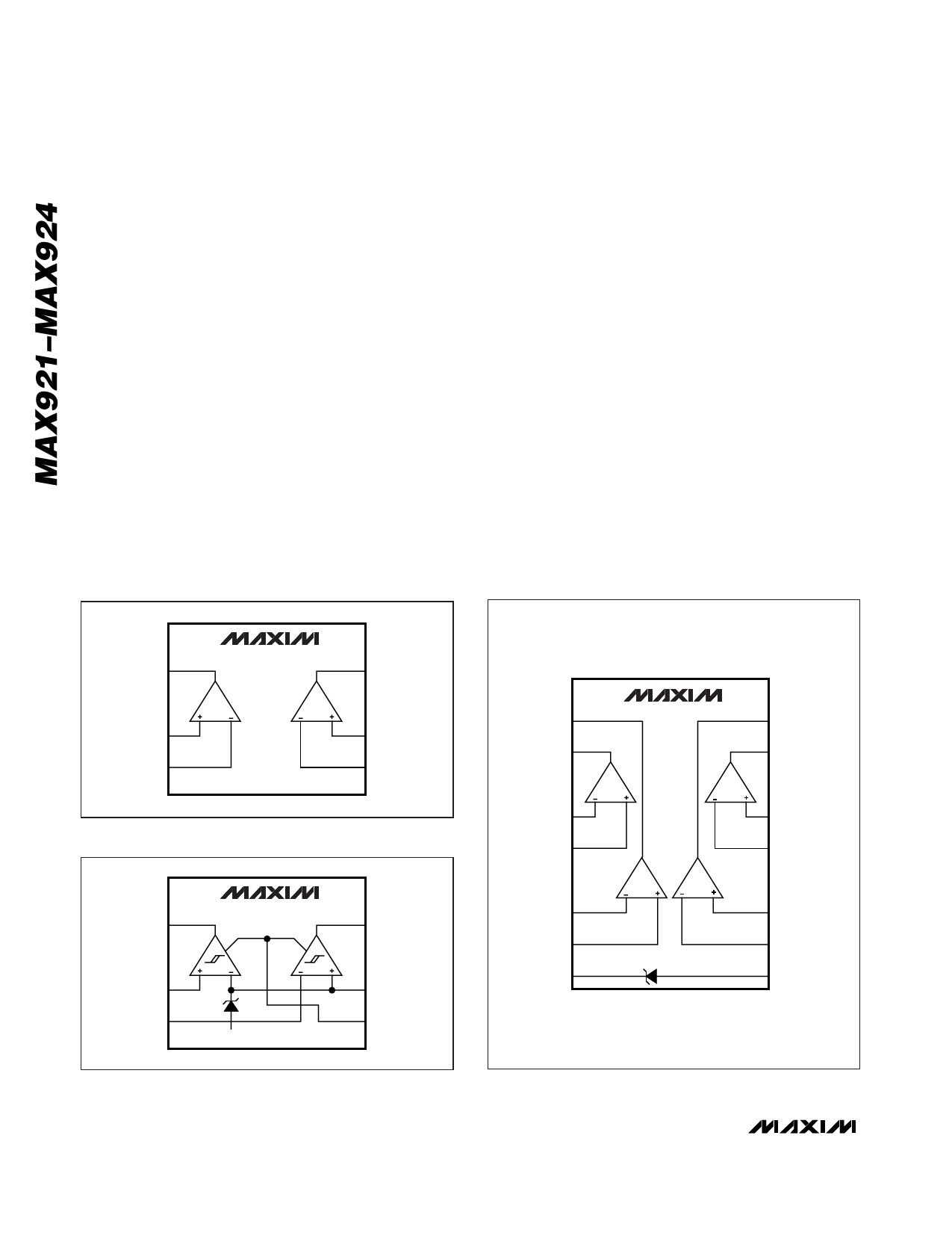
The MAX921–MAX924 comprise various combinations
of a micropower 1.182V reference and a micropower
comparator. The Typical Operating Circuit shows the
MAX921 configuration, and Figures 1a-1c show the
MAX922–MAX924 configurations.
Each comparator continuously sources up to 40mA,
and the unique output stage eliminates crowbar
glitches during output transitions. This makes them
immune to parasitic feedback (which can cause
instability) and provides excellent performance, even
when circuit-board layout is not optimal.
Internal hysteresis in the MAX921 and MAX923 provides
the easiest method for implementing hysteresis. It also
produces faster hysteresis action and consumes much
less current than circuits using external positive feedback.
Power-Supply and Input Signal Ranges
This family of devices operates from a single +2.5V to
+11V power supply. The MAX921 and MAX924 have a
separate ground for the output driver, allowing
operation with dual supplies ranging from ±1.25V to
±5.5V. Connect V- to GND when operating the
MAX921 and the MAX924 from a single supply. The
maximum supply voltage in this case is still 11V.
For proper comparator operation, the input signal can
swing from the negative supply (V-) to within one volt of
the positive supply (V+ – 1V). The guaranteed
common-mode input voltage range extends from V- to
(V+ - 1.3V). The inputs can be taken above and below
the supply rails by up to 300mV without damage.
Operating the MAX921 and MAX924 at ±5V provides
TTL/CMOS compatibility when monitoring bipolar input
signals. TTL compatibility for the MAX922 and MAX923
is achieved by operation from a single +5V supply.
Low-Voltage Operation: V+ = 1V (MAX924 Only)
The guaranteed minimum operating voltage is 2.5V (or
±1.25V). As the total supply voltage is reduced below
2.5V, the performance degrades and the supply
current falls. The reference will not function below
1 OUTA
2 V-
3 INA+
4 INA-
MAX922
OUTB 8
V+ 7
INB+ 6
INB- 5
Figure 1a. MAX922 Functional Diagram
1 OUTB
2 OUTA
3 V+
4 INA-
5 INA+
MAX924
OUTC 16
OUTD 15
GND 14
IND+ 13
IND- 12
1 OUTA
2 V-
3 INA+
4 INB-
MAX923
V-
OUTB 8
V+ 7
REF 6
HYST 5
6 INB-
7 INB+
8 REF
INC+ 11
INC- 10
V- 9
Figure 1b. MAX923 Functional Diagram
Figure 1c. MAX924 Functional Diagram
8 _______________________________________________________________________________________
Share Link: 