MAX9541 データシートの表示(PDF) - Maxim Integrated
部品番号
コンポーネント説明
メーカー
MAX9541 Datasheet PDF : 17 Pages
| |||
MAX9541/MAX9542
Quadruple, 2:1, Mux Amplifiers for
Standard-Definition and VGA Signals
Absolute Maximum Ratings
Supply Voltage
VDD to GND..........................................................-0.3V to +4V
Input Pins, SHDN, A/B............................ (GND - 0.3V) to +4V
Duration of Output Short Circuit to VDD or GND.......Continuous
Continuous Input Current
Input Pins.......................................................................±20mA
Continuous Power Dissipation (TA = +70°C)
16-Pin QSOP (derate 8.3mW/°C above +70°C)..........667mW
Operating Temperature Range.......................... -40°C to +125°C
Junction Temperature.......................................................+150°C
Storage Temperature Range............................. -65°C to +150°C
Lead Temperature (soldering, 10s).................................. +300°C
Stresses beyond those listed under “Absolute Maximum Ratings” may cause permanent damage to the device. These are stress ratings only, and functional operation of the device at these
or any other conditions beyond those indicated in the operational sections of the specifications is not implied. Exposure to absolute maximum rating conditions for extended periods may affect
device reliability.
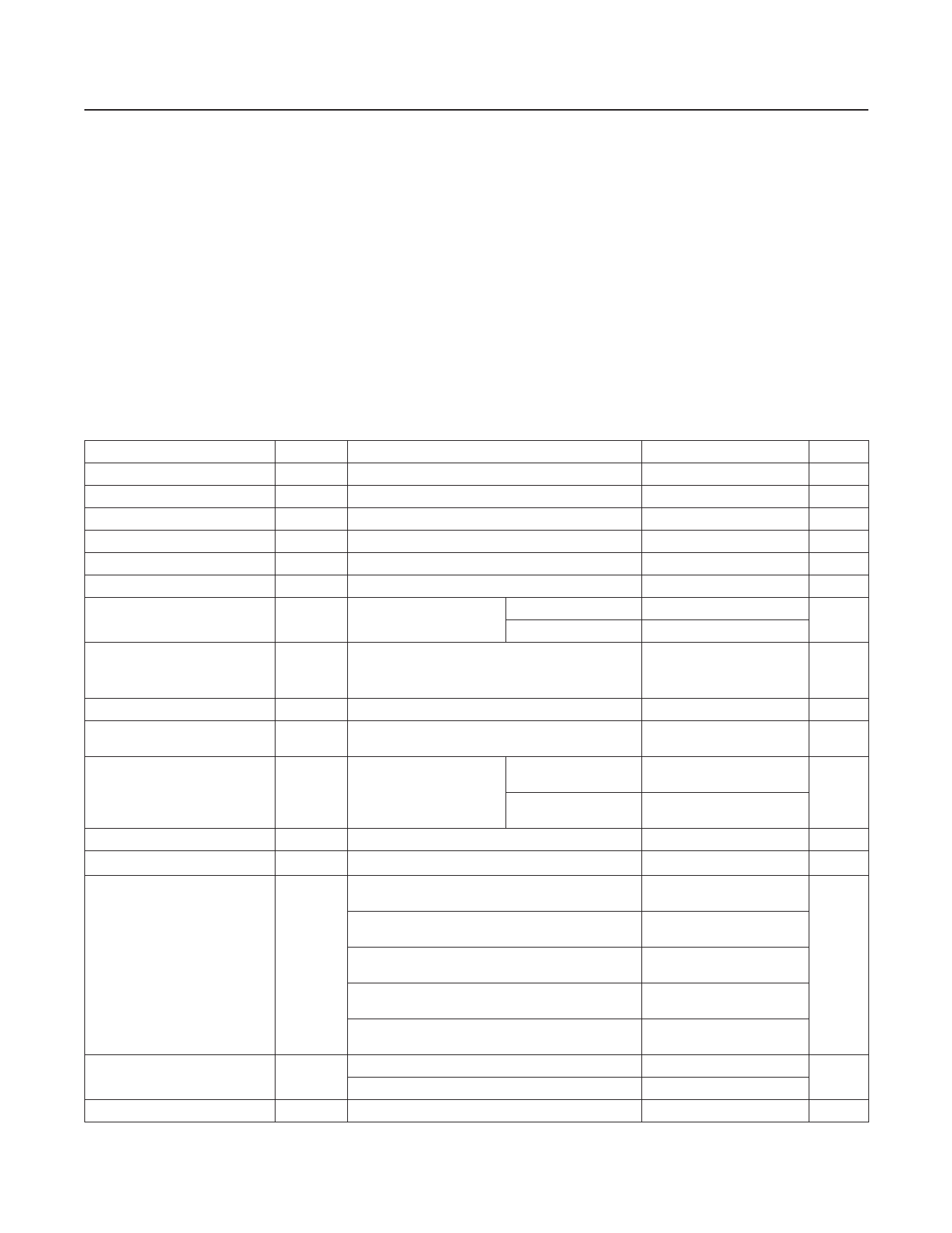
Electrical Characteristics
(VDD = 3.3V, VGND = 0, SHDN = VDD, A/B = VDD, RL = 150Ω to GND, TA = TMIN to TMAX, unless otherwise noted. Typical values
are at TA = +25°C.) (Note 1)
PARAMETER
SYMBOL
CONDITIONS
MIN TYP MAX UNITS
Supply Voltage Range
Quiescent Supply Current
Shutdown Supply Current
Input Voltage
Input Resistance
VDD
IDD
ISHDN
Guaranteed by power-supply rejection test
No load
SHDN = A/B= GND
Unselected input
Unselected input
2.7
3.3
3.6
V
21
45
mA
35
70
µA
VDD/3
V
222
kΩ
Sync-Tip Clamp Level
Input Voltage Range
VCLP
Guaranteed by DC
voltage gain
0.23
0.3
0.39
V
2.7V ≤ VDD ≤ 3.6V
3.0V ≤ VDD ≤ 3.6V
1.05
1.2
VP-P
Sync Crush
Sync-tip clamp; percentage reduction in sync
pulse (0.3VP-P); guaranteed by input clamping
current measurement
2
%
Input Clamping Current
Maximum Input Source
Resistance
DC Voltage Gain (Note 2)
DC Gain Mismatch
AV
RL = 150Ω to GND
(Note 2)
VDD = 2.7V,
0V ≤ VIN ≤ 1.05V
VDD = 3V,
0V ≤ VIN ≤ 1.2V
Guaranteed by DC voltage gain
1
2
µA
300
Ω
1.96
2
2.04
V/V
1.96
2
2.04
-2
+2
%
Output Level
Output Voltage Swing
Output Short-Circuit Current
Output Resistance
Measured at VOUT, CIN_ = 0.1µF to GND
0.218 0.3
Measured at output, VDD = 2.7V, VIN = VCLP
to (VCLP +1.05V), RL = 150Ω to -0.2V
2.1
Measured at output, VDD = 2.7V, VIN = VCLP
to (VCLP +1.05V), RL = 150Ω to VDD/2
2.1
Measured at output, VDD = 3.0V, VIN = VCLP
to (VCLP +1.2V), RL = 150Ω to -0.2V
2.4
Measured at output, VDD = 3.0V, VIN = VCLP
to (VCLP +1.2V), RL = 150Ω to VDD/2
2.4
Measured at output, VDD = 3.135V, VIN = VCLP
to (VCLP +1.05V), RL = 75Ω to -0.2V
2.1
Short to GND (sourcing)
140
Short to VDD (sinking)
70
ROUT VOUT = 1.5V, -10mA ≤ ILOAD ≤ +10mA
0.2
0.39
V
VP-P
mA
Ω
www.maximintegrated.com
Maxim Integrated │ 2
Share Link: 