MBM29LV008BA-12 гғҮгғјгӮҝгӮ·гғјгғҲгҒ®иЎЁзӨәпјҲPDFпјү - Fujitsu
йғЁе“Ғз•ӘеҸ·
гӮігғігғқгғјгғҚгғігғҲиӘ¬жҳҺ
гғЎгғјгӮ«гғј
MBM29LV008BA-12 Datasheet PDF : 51 Pages
| |||
MBM29LV008TA-70/-90/-12/MBM29LV008BA-70/-90/-12
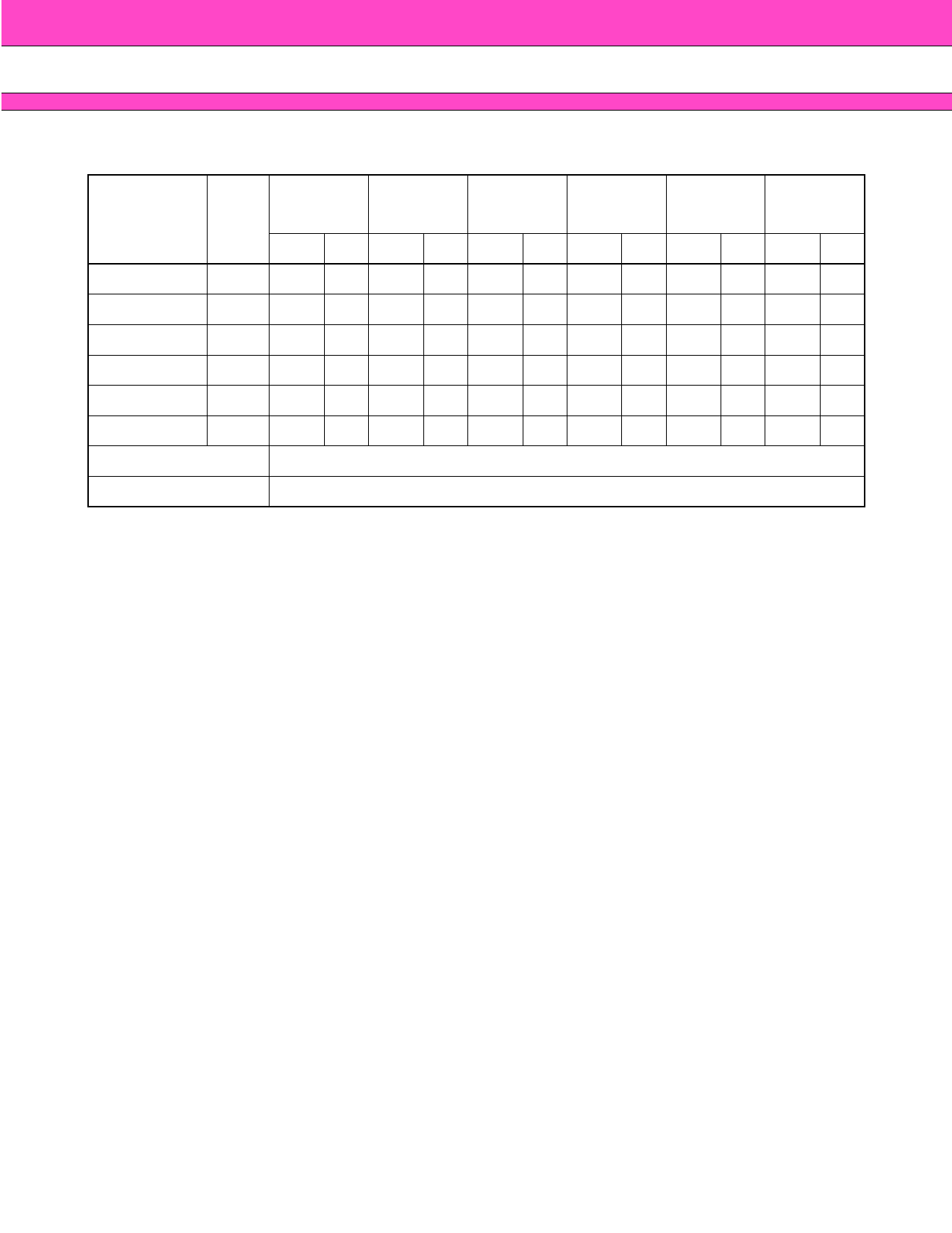
Table 6 MBM29LV008TA/008BA Standard Command Definitions
Command
Sequence
Bus
Write
Cycles
First Bus Second Bus Third Bus
Write Cycle Write Cycle Write Cycle
Fourth Bus
Read/Write
Cycle
Fifth Bus
Write Cycle
Sixth Bus
Write Cycle
ReqвҖҷd Addr. Data Addr. Data Addr. Data Addr. Data Addr. Data Addr. Data
Read/Reset
1 XXXH F0H вҖ” вҖ” вҖ” вҖ” вҖ” вҖ” вҖ” вҖ” вҖ” вҖ”
Read/Reset
3 555H AAH 2AAH 55H 555H F0H RA RD вҖ” вҖ” вҖ” вҖ”
Autoselect
3 555H AAH 2AAH 55H 555H 90H вҖ” вҖ” вҖ” вҖ” вҖ” вҖ”
Program
4 555H AAH 2AAH 55H 555H A0H PA PD вҖ” вҖ” вҖ” вҖ”
Chip Erase
6 555H AAH 2AAH 55H 555H 80H 555H AAH 2AAH 55H 555H 10H
Sector Erase
6 555H AAH 2AAH 55H 555H 80H 555H AAH 2AAH 55H SA 30H
Sector Erase Suspend Erase can be suspended during sector erase with Addr. (вҖңHвҖқ or вҖңLвҖқ). Data (B0H)
Sector Erase Resume Erase can be resumed after suspend with Addr. (вҖңHвҖқ or вҖңLвҖқ). Data (30H)
Notes: 1. Address bits A11 to A19 = X = вҖңHвҖқ or вҖңLвҖқ for all address commands except or Program Address (PA) and
Sector Address (SA)
2. Bus operations are defined in Table 2.
3. RA = Address of the memory location to be read
PA = Address of the memory location to be programmed
Addresses are latched on the falling edge of the write pulse.
SA = Address of the sector to be erased. The combination of A19, A18, A17, A16, A15, A14, and A13 will
uniquely select any sector.
4. RD = Data read from location RA during read operation.
PD = Data to be programmed at location PA. Data is latched on the falling edge of write pulse.
5. Both Read/Reset commands are functionally equivalent, resetting the device to the read mode.
14
Share Link: 