MC14LC5447DW データシートの表示(PDF) - Motorola => Freescale
部品番号
コンポーネント説明
メーカー
MC14LC5447DW Datasheet PDF : 12 Pages
| |||
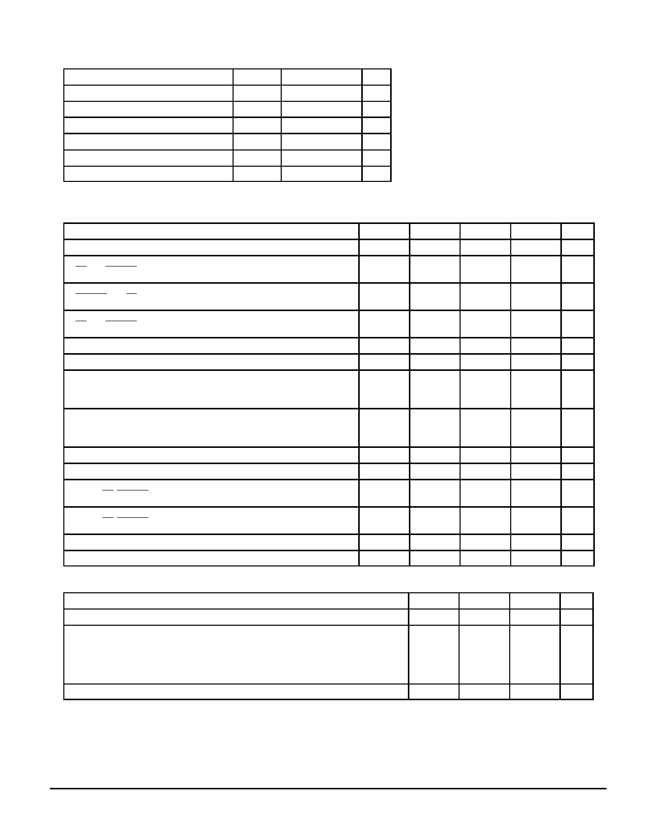
ABSOLUTE MAXIMUM RATINGS
(Voltages referenced to GND, except where noted)
Rating
DC Supply Voltage
Input Voltage, All Pins
DC Current Drain Per Pin
Power Dissipation
Operating Temperature Range
Storage Temperature Range
Symbol
VDD
Vin
I
PD
TA
Tstg
Value
Unit
– 0.5 to + 6.0
V
– 0.5 to VDD + 0.5 V
± 10
mA
20
mW
0 to + 70
°C
– 40 to + 150
°C
This device contains circuitry to protect the
inputs against damage due to high static volt-
ages or electric fields. However, it is advised that
normal precautions be taken to avoid applica-
tions of any voltage higher than maximum rated
voltages to this high impedance circuit. For
proper operation it is recommended that Vin and
Vout be constrained to the range VSS ≤ (Vin or
Vout) ≤ VDD.
Reliability of operation is enhanced if unused
inputs are tied to an appropriate logic voltage
level (e.g., either VSS or VDD).
ELECTRICAL CHARACTERISTICS
(All polarities referenced to VSS = 0 V, VDD = + 5 V ± 10%, unless otherwise noted, TA = 0 to + 70°C)
Parameter
Symbol
Min
Typ
Max
Unit
DC Supply Voltage
Supply Current (All Output Pins Unloaded) (See Figure 1)
RT = 0, PWRUP = 1, XTAL = 3.58 MHz
VDD
3.5
5
IDD
—
2.4
6
V
3
mA
Supply Current (All Output Pins Unloaded) (See Figure 1)
PWRUP = 0, RT = Don’t Care, XTAL = 3.58 MHz
IDD
—
4.0
5.5
mA
Standby Current (All Output Pins Unloaded) (See Figure 1)
RT = 1, PWRUP = 1
ISTBY
—
—
1
µA
Input Voltage 0 Level (CLKSIN, OSCin)
VIL
—
—
VDD x 0.3 V
Input Voltage 1 Level (CLKSIN, OSCin)
VIH
VDD x 0.7
—
—
V
Output Voltage High: VDD = 5 V (DOR, DOC, OSCout)
VOH
—
IOH = 40 µA
2.4
IOH ≤ 1 µA
4.95
—
V
Output Voltage Low: VDD = 5 V (DOR, DOC, OSCout)
VOL
—
IOL = 1.6 mA
IOL ≤ 1 µA
—
V
0.4
0.05
Input Leakage Current (OSCin, CLKSIN, PWRUP, RT, RDI1, and RDI2)
Iin
—
—
±1
µA
Output Voltage Low: VDD = 5 V (RDO, RT, CDO) IOL = 2.0 mA
VOL
—
—
0.4
V
Input Threshold Voltage Positive Going: VDD = 5 V
(RDI1, RT, PWRUP) (See Figure 3)
VT+
2.5
2.75
3.0
V
Input Threshold Voltage Negative Going: VDD = 5 V
(RDI1, RT, PWRUP) (See Figure 3)
VT–
2.0
2.3
2.6
V
RDI2 Threshold
TIP/RING Input dc Resistance
RD2VT
1.0
1.1
1.2
V
Rin
—
250
—
kΩ
ANALOG CHARACTERISTICS (VDD = + 5 V, TA = + 25°C, unless otherwise noted, 0 dBm = 0.7746 Vrms @ 600 Ω)
Characteristic
Min
Typ
Max
Input Sensitivity: TIP and RING (Pins 1 and 2, VDD = + 5 V)
Band–Pass Filter (BPF)
Frequency Response (Relative to 1700 Hz @ 0 dBm)
– 40
– 45
—
60 Hz
—
– 64
—
500 Hz
—
–4
—
2700 Hz
—
–3
—
≥ 3300 Hz
—
– 34
—
Carrier Detect Sensitivity
—
– 48
—
Unit
dBm
dB
dBm
MC14LC5447
2
MOTOROLA
Share Link: 