MC74VHCT541A データシートの表示(PDF) - Motorola => Freescale
部品番号
コンポーネント説明
メーカー
MC74VHCT541A Datasheet PDF : 6 Pages
| |||
MOTOROLA
SEMICONDUCTOR TECHNICAL DATA
Octal Bus Buffer
The MC74VHCT541A is an advanced high speed CMOS octal bus buffer
fabricated with silicon gate CMOS technology. It achieves high speed
operation similar to equivalent Bipolar Schottky TTL while maintaining
CMOS low power dissipation.
The MC74VHCT541A is a noninverting, 3–state, buffer/line driver/line
receiver. When either OE1 or OE2 is high, the terminal outputs are in the
high impedance state.
The VHCT inputs are compatible with TTL levels. This device can be used
as a level converter for interfacing 3.3V to 5.0V, because it has full 5V CMOS
level output swings.
The VHCT541A input and output (when disabled) structures provide
protection when voltages between 0V and 5.5V are applied, regardless of
the supply voltage. These input and output structures help prevent device
destruction caused by supply voltage – input/output voltage mismatch,
battery backup, hot insertion, etc.
• High Speed: tPD = 5.4ns (Typ) at VCC = 5V
• Low Power Dissipation: ICC = 4µA (Max) at TA = 25°C
• TTL–Compatible Inputs: VIL = 0.8V; VIH = 2.0V
• Power Down Protection Provided on Inputs and Outputs
• Balanced Propagation Delays
• Designed for 4.5V to 5.5V Operating Range
• Low Noise: VOLP = 1.6V (Max)
• Pin and Function Compatible with Other Standard Logic Families
• Latchup Performance Exceeds 300mA
• ESD Performance: HBM > 2000V; Machine Model > 200V
• Chip Complexity: 134 FETs or 33.5 Equivalent Gates
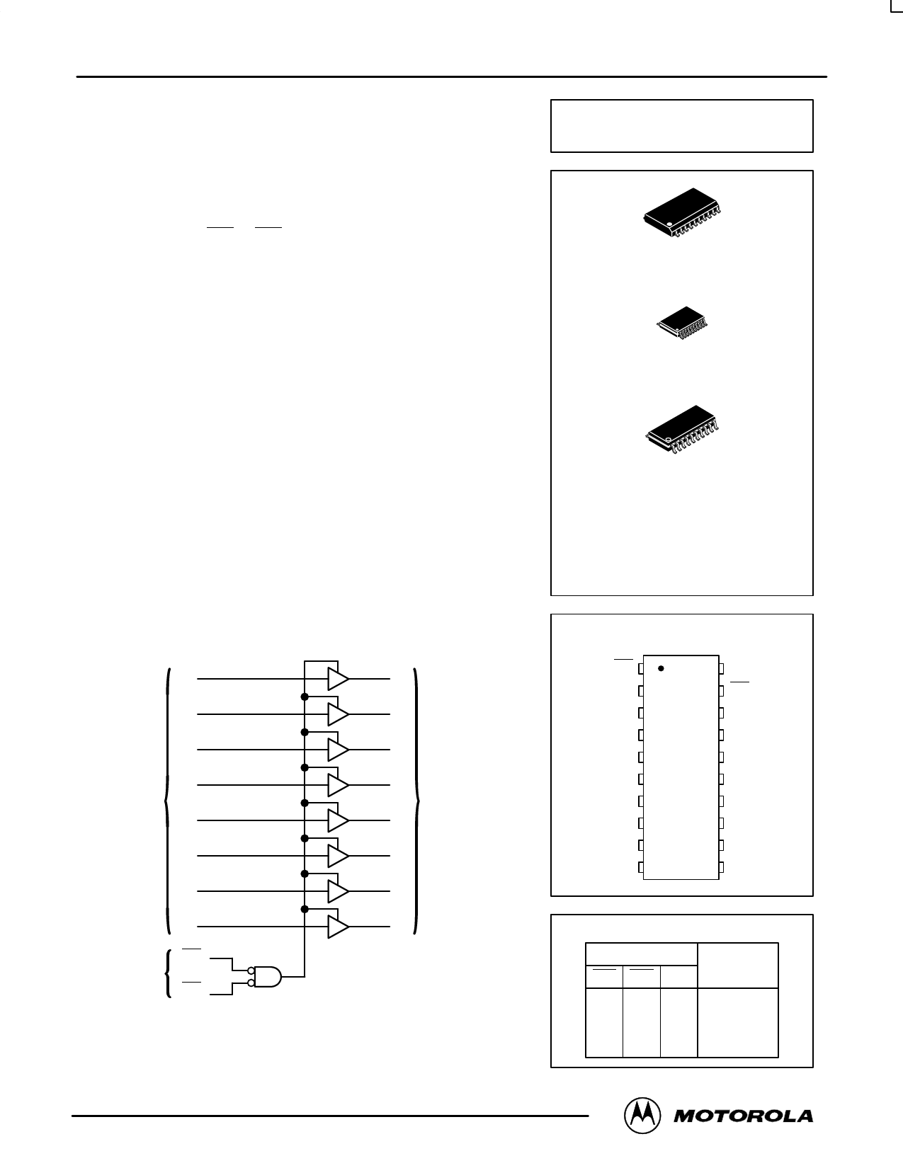
DATA
INPUTS
OUTPUT
ENABLES
2
A1
3
A2
4
A3
5
A4
6
A5
7
A6
8
A7
9
A8
1
OE1
OE2 19
LOGIC DIAGRAM
18
Y1
17
Y2
16
Y3
15
Y4
14
Y5
NONINVERTING
OUTPUTS
13
Y6
12
Y7
11
Y8
MC74VHCT541A
DW SUFFIX
20–LEAD SOIC PACKAGE
CASE 751D–04
DT SUFFIX
20–LEAD TSSOP PACKAGE
CASE 948E–02
M SUFFIX
20–LEAD SOIC EIAJ PACKAGE
CASE 967–01
ORDERING INFORMATION
MC74VHCTXXXADW SOIC
MC74VHCTXXXADT TSSOP
MC74VHCTXXXAM SOIC EIAJ
PIN ASSIGNMENT
OE1 1
A1 2
A2 3
A3 4
A4 5
A5 6
A6 7
A7 8
A8 9
GND 10
20 VCC
19 OE2
18 Y1
17 Y2
16 Y3
15 Y4
14 Y5
13 Y6
12 Y7
11 Y8
FUNCTION TABLE
Inputs
OE1 OE2 A
Output Y
L
L
L
L
L
L
H
H
HXX
Z
XHX
Z
6/97
© Motorola, Inc. 1997
1
REV 0
Share Link: 