MCM6229BB データシートの表示(PDF) - Motorola => Freescale
部品番号
コンポーネント説明
メーカー
MCM6229BB Datasheet PDF : 8 Pages
| |||
CAPACITANCE (f = 1.0 MHz, dV = 3.0 V, TA = 25°C, Periodically Sampled Rather Than 100% Tested)
Characteristic
Symbol Typ
Input Capacitance
All Inputs Except Clocks and DQs
Cin
4
E, G, and W Cck
5
I/O Capacitance
DQ CI/O
5
Max Unit
6
pF
8
8
pF
AC OPERATING CONDITIONS AND CHARACTERISTICS
(VCC = 5.0 V ± 10%, TA = 0 to + 70°C, Unless Otherwise Noted)
Input Pulse Levels . . . . . . . . . . . . . . . . . . . . . . . . . . . . . . . . . 0 to 3.0 V
Input Rise/Fall Time . . . . . . . . . . . . . . . . . . . . . . . . . . . . . . . . . . . . 2 ns
Input Timing Measurement Reference Level . . . . . . . . . . . . . . . 1.5 V
Output Timing Measurement Reference Level . . . . . . . . . . . . . 1.5 V
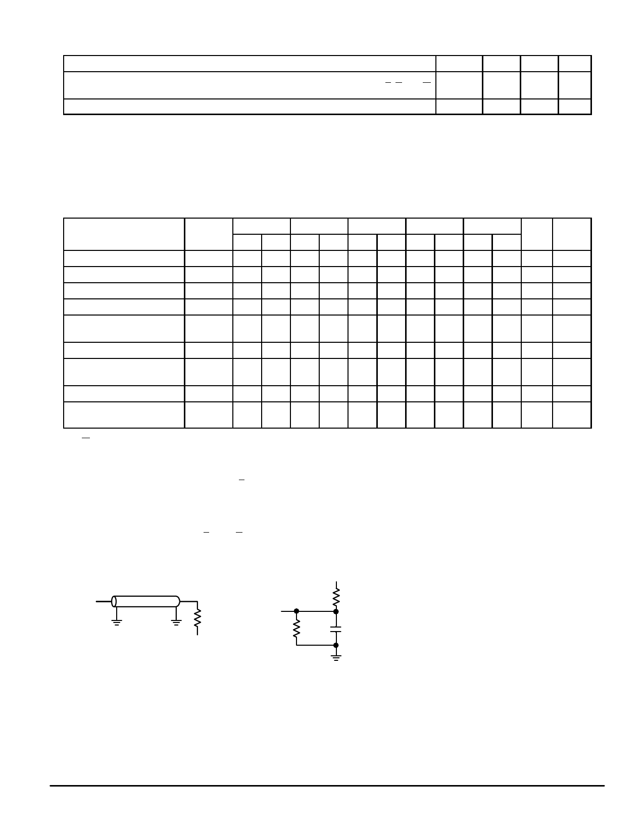
Output Load . . . . . . . . . . . . . . . . . . . . . . . . . . . . . . . . . . See Figure 1a
READ CYCLE TIMING (See Notes 1, 2, and 3)
6229BB–15 6229BB–17 6229BB–20 6229BB–25 6229BB–35
Parameter
Symbol Min Max Min Max Min Max Min Max Min Max Unit Notes
Read Cycle Time
tAVAV
15 — 17 — 20 — 25 — 35 —
ns
3
Address Access Time
tAVQV
— 15 — 17 — 20 — 25 — 35
ns
Enable Access Time
tELQV
— 15 — 17 — 20 — 25 — 35
ns
4
Output Enable Access Time
tGLQV
—
6
—
7
—
7
—
8
—
8
ns
Output Hold from Address
Change
tAXQX
3
—
3
—
3
—
3
—
3
—
ns
Enable Low to Output Active
tELQX
5
—
5
—
5
—
5
—
5
—
ns 5, 6, 7
Output Enable Low to Output tGLQX
0
—
0
—
0
—
0
—
0
—
ns 5, 6, 7
Active
Enable High to Output High–Z tEHQZ
0
6
0
7
0
7
0
8
0
8
ns 5, 6, 7
Output Enable High to Output tGHQZ
0
6
0
7
0
7
0
8
0
8
ns 5, 6, 7
High–Z
NOTES:
1. W is high for read cycle.
2. Product sensitivities to noise require proper grounding and decoupling of power supplies as well as minimization or elimination of bus con-
tention conditions during read and write cycles.
3. All timings are referenced from the last valid address to the first transitioning address.
4. Addresses valid prior to or coincident with E going low.
5. At any given voltage and temperature, tEHQZ max is less than tELQX min, and tGHQZ max is less than tGLQX min, both for a given device
and from device to device.
6. Transition is measured ± 500 mV from steady–state voltage with load of Figure 1b.
7. This parameter is sampled and not 100% tested.
8. Device is continuously selected (E ≤ VIL, G ≤ VIL).
OUTPUT
Z0 = 50 Ω
OUTPUT
RL = 50 Ω
255 Ω
VL = 1.5 V
+5 V
480 Ω
5 pF
(a)
(b)
Figure 1. AC Test Loads
TIMING LIMITS
The table of timing values shows either a
minimum or a maximum limit for each param-
eter. Input requirements are specified from
the external system point of view. Thus, ad-
dress setup time is shown as a minimum
since the system must supply at least that
much time. On the other hand, responses
from the memory are specified from the de-
vice point of view. Thus, the access time is
shown as a maximum since the device never
provides data later than that time.
MOTOROLA FAST SRAM
MCM6229BB
3
Share Link: 