MN12511 データシートの表示(PDF) - Panasonic Corporation
部品番号
コンポーネント説明
メーカー
MN12511 Datasheet PDF : 9 Pages
| |||
Microcontroller Peripheral LSIs
s Pin Descriptions (continued)
Pin No. Symbol
I/O
19
D5
O
20
D4
O
21
D3
O
22
D2
O
23
D1
O
24
D0
O
Description
High-voltage output 5
High-voltage output 4
High-voltage output 3
High-voltage output 2
High-voltage output 1
High-voltage output 0
MN12511
s Operational Description
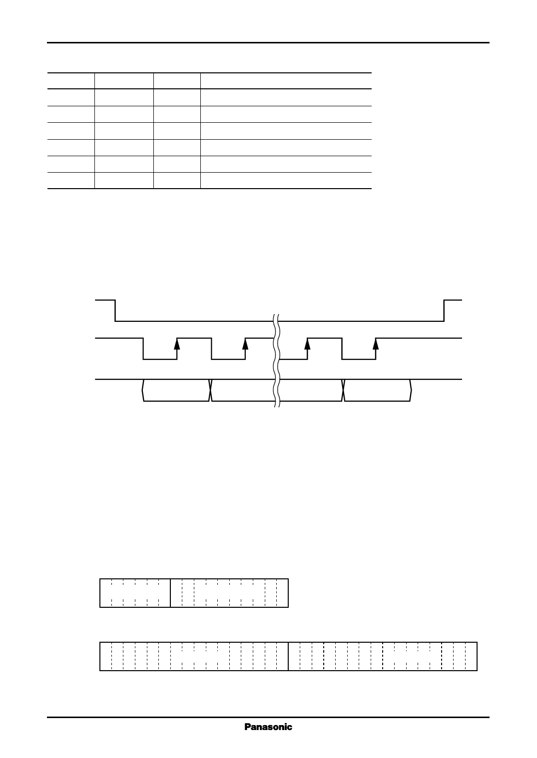
• Transfer timing
The figure below shows the input timing for the NCE, NSCK, and NSDI pins during data transfers.
NCE
NSCK
NSDI
D15
D14
D1
D0
NSDI is acquired on the rising edge of NSCK.
NSDO is output on the falling edge of NSCK.
• Transfer Format
The following transfer formats could be considered as the data format for data transfer from the system
microcontroller.
Note that other transfer formats are possible, depending on the requirements of the particular application.
Example: For use with a 6-grid × 10-segment display (Using a single MN12511)
6 grid-bit
10 segment-bit
Example: For use with a 15-grid × 11-segment display (Using two MN12511 chips)
*
15 grid-bit
Note) *: Bits marked with an asterisk are unused.
* ****
11 segment-bit
3
Share Link: 