MN12511 データシートの表示(PDF) - Panasonic Corporation
部品番号
コンポーネント説明
メーカー
MN12511 Datasheet PDF : 9 Pages
| |||
Microcontroller Peripheral LSIs
MN12511
s Electrical Characteristics (continued)
Note) (continued)
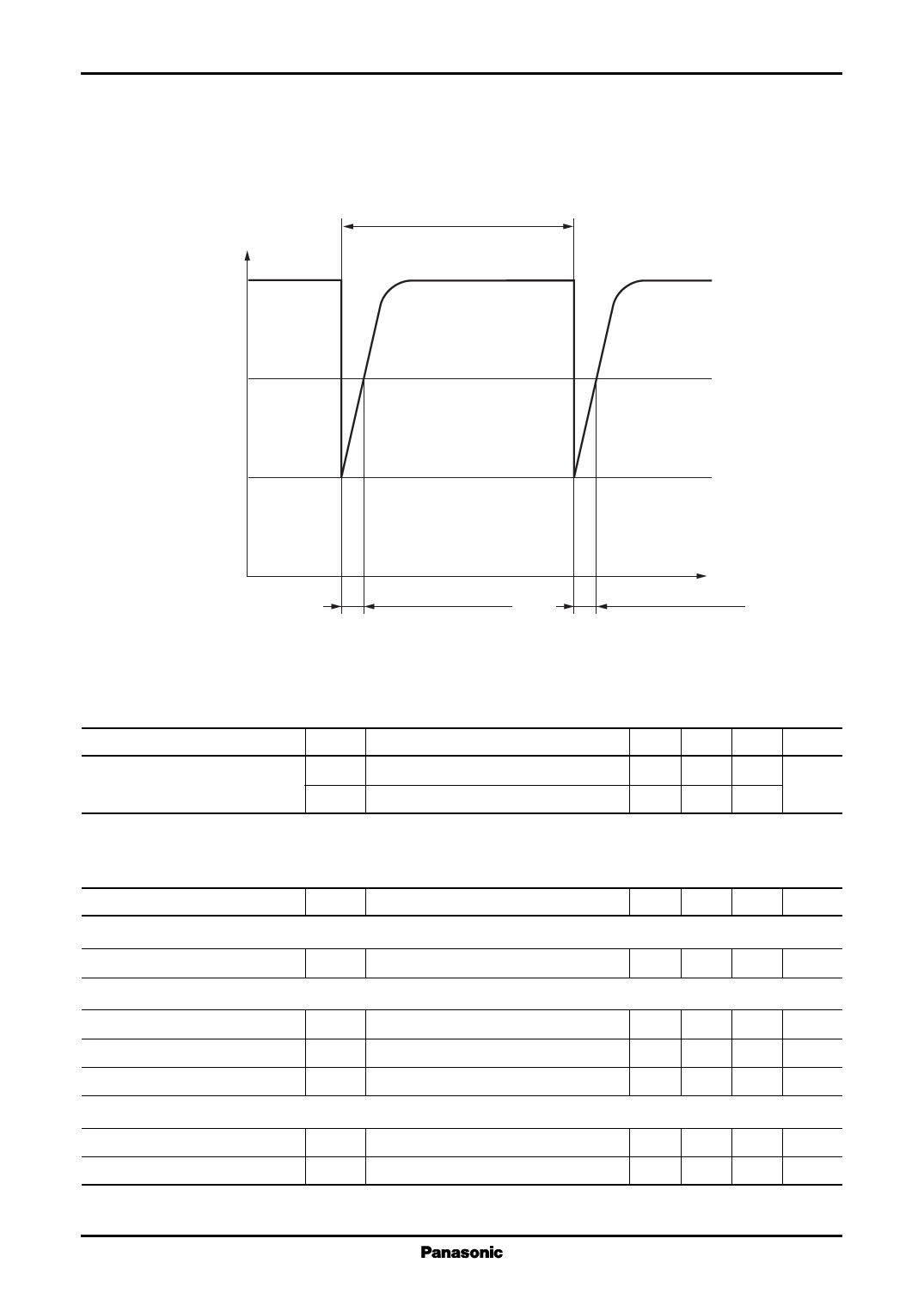
4. The rating for capacitance coupled spike noise that exceeds the absolute maximum rating of −40 V and that occurs at most
once in any of the display cycles is defined as shown below.
Period T
V
−30 V
−40 V
−50 V
No more than 50 µs
T
No more than 50 µs
5. Insert a capacitor of at least 0.1 µF between VDD and VSS as close as possible to the LSI pins.
2. Operating Conditions at VSS = 0 V, Ta = −10 °C to 70 °C
Parameter
Symbol
Conditions
Min Typ Max Unit
Supply Voltage
VDD
4.5 5.0 5.5 V
VPP Potential difference between VDD and VPP. 35
3. DC Characteristics at VSS = 0 V, Ta = −10 °C to 70 °C
Parameter
Symbol
Conditions
1) Supply current
Operating supply current
IDD
2) Input pins NCE, OE, NSCK, and NSDI (Schmitt inputs)
High-level input voltage
VIH1
Low-level input voltage
Input leakage current
VIL1
ILK1
VIN = 0 to 5 V
3) The NSDO output pin
High-level output voltage
Low-level output voltage
VOH1 IOH1 = − 0.5 mA
VOL1 IOL2 = 0.5 mA
Min Typ Max Unit
3 10 mA
0.7VDD VDD
V
VSS 0.2VDD V
±10 µA
4.5
V
0.5 V
5
Share Link: 