MT46V128M4 データシートの表示(PDF) - Micron Technology
部品番号
コンポーネント説明
メーカー
MT46V128M4 Datasheet PDF : 91 Pages
| |||
512Mb: x4, x8, x16 DDR SDRAM
Features
Double Data Rate (DDR) SDRAM
MT46V128M4 – 32 Meg x 4 x 4 banks
MT46V64M8 – 16 Meg x 8 x 4 banks
MT46V32M16 – 8 Meg x 16 x 4 banks
Features
• VDD = +2.5V ±0.2V, VDDQ = +2.5V ±0.2V
• VDD = +2.6V ±0.1V, VDDQ = +2.6V ±0.1V (DDR400)
• Bidirectional data strobe (DQS) transmitted/
received with data, i.e., source-synchronous data
capture (x16 has two – one per byte)
• Internal, pipelined double-data-rate (DDR)
architecture; two data accesses per clock cycle
• Differential clock inputs (CK and CK#)
• Commands entered on each positive CK edge
• DQS edge-aligned with data for READs; center-
aligned with data for WRITEs
• DLL to align DQ and DQS transitions with CK
• Four internal banks for concurrent operation
• Data mask (DM) for masking write data
(x16 has two – one per byte)
• Programmable burst lengths: 2, 4, or 8
• Auto refresh
– 64ms, 8192-cycle(Commercial and industrial)
– 16ms, 8192-cycle (Automotive)
• Self refresh (not available on AT devices)
• Longer-lead TSOP for improved reliability (OCPL)
• 2.5V I/O (SSTL_2 compatible)
• Concurrent auto precharge option is supported
• tRAS lockout supported (tRAP = tRCD)
Options
Marking
• Configuration
– 128 Meg x 4 (32 Meg x 4 x 4 banks)
128M4
– 64 Meg x 8 (16 Meg x 8 x 4 banks)
64M8
– 32 Meg x 16 (8 Meg x 16 x 4 banks)
32M16
• Plastic package
– 66-pin TSOP
TG
– 66-pin TSOP (Pb-free)
P
– 60-ball FBGA (10mm x 12.5mm)
FN
– 60-ball FBGA (10mm x 12.5mm) (Pb-free) BN
• Timing – cycle time
– 5ns @ CL = 3 (DDR400B)
-5B
– 6ns @ CL = 2.5 (DDR333) (FBGA only)
-6
– 6ns @ CL = 2.5 (DDR333) (TSOP only)
– 7.5ns @ CL = 2 (DDR266)
– 7.5ns @ CL = 2 (DDR266A)
– 7.5ns @ CL = 2.5 (DDR266B)
-6T
-75E1
-75Z1
-751
• Self refresh
– Standard
None
– Low-power self refresh
L
• Temperature rating
– Commercial (0°C to +70°C)
None
– Industrial (–40°C to +85°C)
IT
– Automotive (–40°C to +105°C)
AT
• Revision
– x4, x8
:D1
– x4, x8, x16
:F
Notes: 1. End of life.
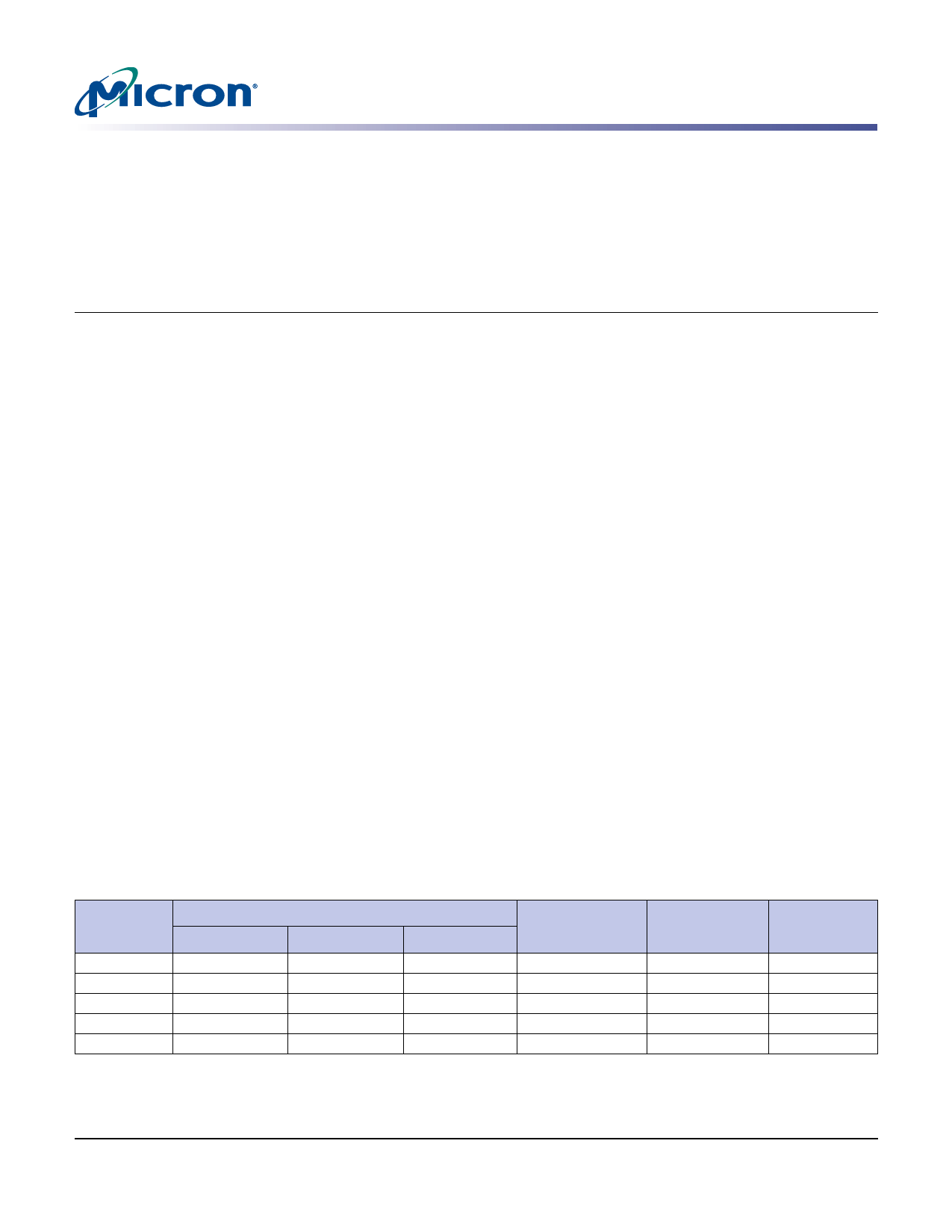
Table 1:
Key Timing Parameters
CL = CAS (READ) latency; data-out window is MIN clock rate with 50% duty cycle at CL = 2, CL = 2.5, or CL = 3
Speed
Grade
-5B
-6
6T
-75E/-75Z
-75
CL = 2
133
133
133
133
100
Clock Rate (MHz)
CL = 2.5
167
167
167
133
133
CL = 3
200
n/a
n/a
n/a
n/a
Data-Out
Window
1.6ns
2.1ns
2.0ns
2.5ns
2.5ns
Access
Window
±0.70ns
±0.70ns
±0.70ns
±0.75ns
±0.75ns
DQS–DQ
Skew
+0.40ns
+0.40ns
+0.45ns
+0.50ns
+0.50ns
PDF: 09005aef80a1d9d4/Source: 09005aef82a95a3a
512Mb_DDR_x4x8x16_D1.fm - 512Mb DDR: Rev. N; Core DDR Rev. B 2/09 EN
1
Micron Technology, Inc., reserves the right to change products or specifications without notice.
©2000 Micron Technology, Inc. All rights reserved.
Share Link: 