PI5V330 データシートの表示(PDF) - Pericom Semiconductor Corporation
部品番号
コンポーネント説明
メーカー
PI5V330 Datasheet PDF : 8 Pages
| |||
PI5V330
Low On-Resistance Wideband/Video
Quad 2-Channel Mux/DeMux
Maximum Ratings
(Above which the useful life may be impaired. For user guidelines, not tested.)
Storage Temperature...........................................................–65°C to +150°C
Ambient Temperature with Power Applied..........................–40°C to +85°C
Supply Voltage to Ground Potential (Inputs & VCC Only)...–0.5V to +7.0V
Supply Voltage to Ground Potential (Outputs & D/O Only).–0.5V to +7.0V
DC Input Voltage...................................................................–0.5V to +7.0V
DC Output Current.............................................................................120mA
Note:
Stresses greater than those listed under MAXIMUM RAT-
INGS may cause permanent damage to the device. This is
a stress rating only and functional operation of the device
at these or any other conditions above those indicated in the
operational sections of this specification is not implied. Ex-
posure to absolute maximum rating conditions for extended
periods may affect reliability.
Power Dissipation..................................................................................0.5W
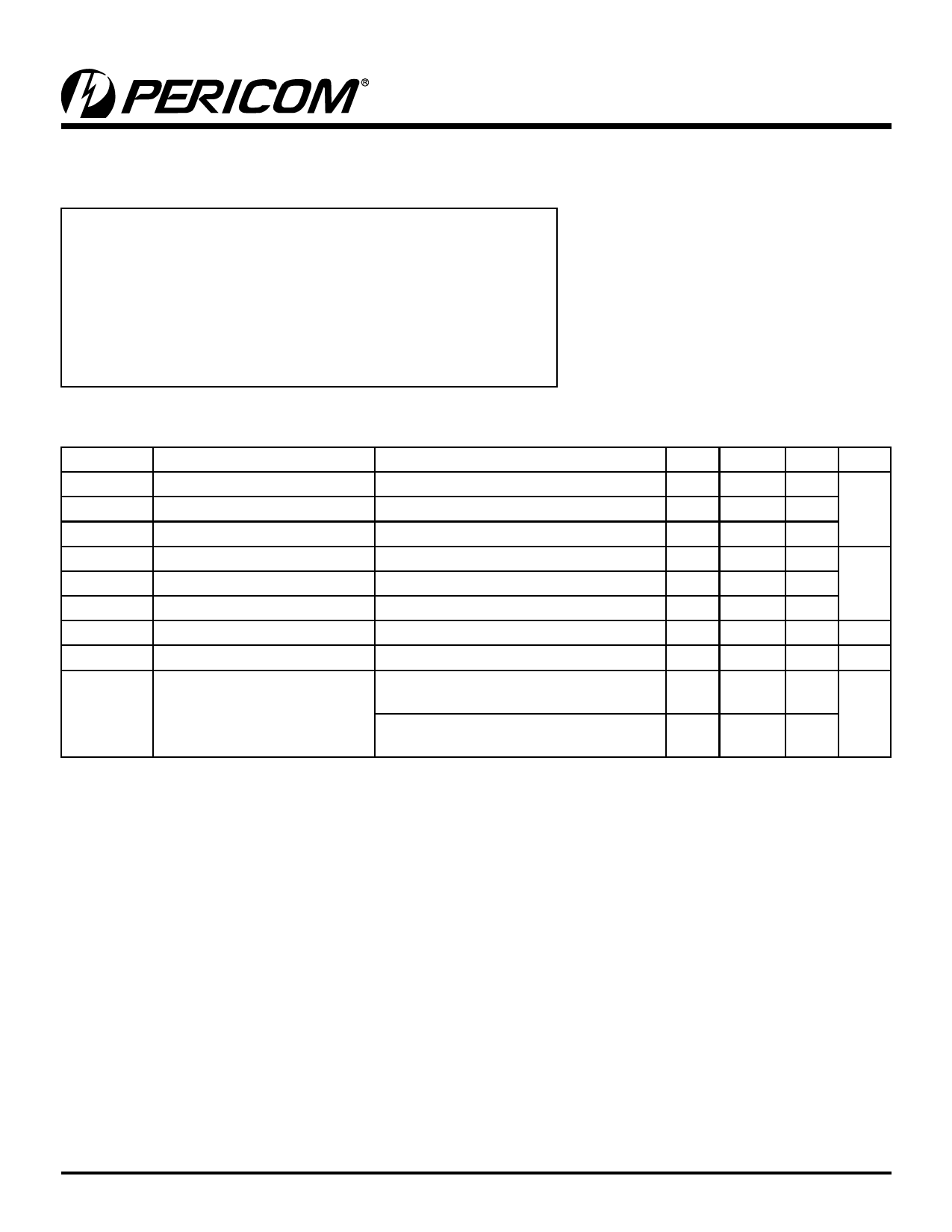
DC Electrical Characteristics (Over the Operating Range, TA = –40°C to +85°C, VCC = 5V ±5%)
Parameters
Description
Test Conditions(1)
Min. Typ.(2) Max. Units
VANALOG Analog Signal Range
0
2.0
VIH
Input HIGH Voltage
VIL
Input LOW Voltage
IIH
Input HIGH Current
Guaranteed Logic HIGH Level
Guaranteed Logic LOW Level
VCC = Max., VIN = VCC
2.0
V
–0.5
0.8
±1
IIL
Input LOW Current
VCC = Max., VIN = GND
IO
Analog Output Leakage Current 0 ≤ S1, S2 or D ≤ VCC, Switch OFF
VIK
Clamp Diode Voltage
VCC = Min., IIN = -18mA
VH
Input Hysteresis at Control Pins
-0.7 -1.2
150
±1 µA
±1
V
mV
RON
Switch On-Resistance(3)
VCC = Min., VIN = 1.0V,
ION = 13mA
VCC = Min., VIN = 2.0V,
ION = 26mA
5
7
Ω
7
10
Notes:
1. For Max. or Min. conditions, use appropriate value specified under Electrical Characteristics for the applicable device type.
2. Typical values are at VCC = 5.0V, TA = 25°C ambient and maximum loading.
3. Measured by the voltage drop between S1, S2, and D I/O pins at indicated current through the switch. On-Resistance is determined by the
lower of the voltages on the S1, S2, and D I/O pins.
13-0017
2
PS7032I
01/14/13
Share Link: 