R8A20210BG データシートの表示(PDF) - Renesas Electronics
部品番号
コンポーネント説明
メーカー
R8A20210BG Datasheet PDF : 14 Pages
| |||
R8A20211BG/R8A20210BG (MARIE_Blade)
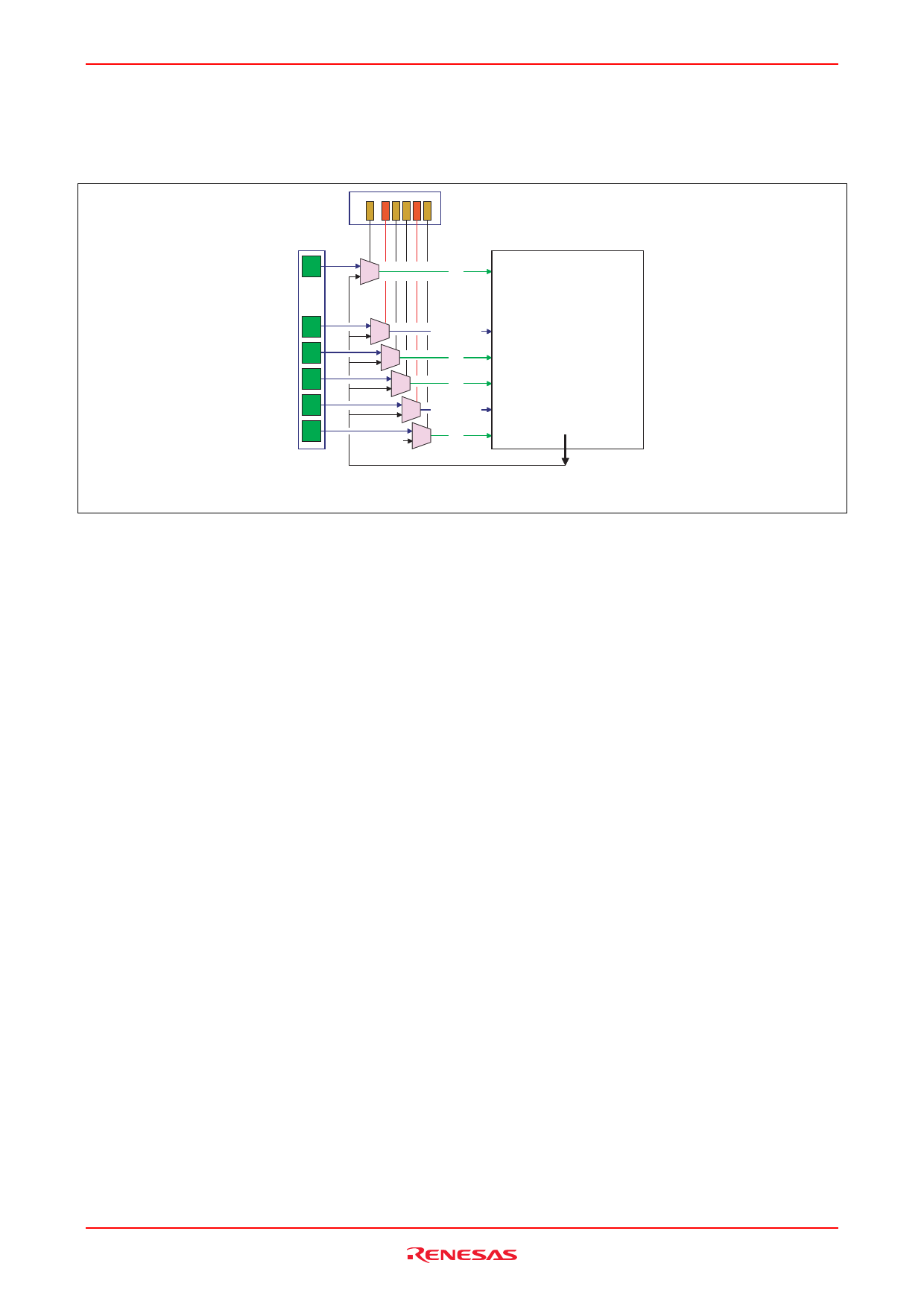
8. Write Mask Register
The Write Mask Register (WMR) controls bits that participate in the Write TCAM operation. The WMR mask has
the same bit width as that of corresponding CAM DQ array.
Also, this register is valid only during Write TCAM. When writing to the 9 M Mats simultaneously (Greedy
Operation), MARIE_Blade uses the mask register that is shared between MAT A and Mat B (Greedy Write).
Write Mask
1 01101
DQ
Write Data
DQ
Former value
DQ
DQ
Former value
DQ
TCAM DQ Array
The WMR bit width is the same as that of DQ.
1-bit WMR masks 1-bit DQ.
Figure 5 Masked Write TCAM
9. Address Source and Data Source
A couple of different sources can be selected to write addresses and/or data into the DQ array. Two possible sources
for the address input are the DQ input pin and the Address Source Register (ASR). Three possible sources for data
input are the DQ input pin, the Data Source Register (DSR), or the Load Data Register (LDR).
⎯ Address Source Register (ASR)
There are two sources to input entry addresses to the DQ array: The DQ pin and ASR. An entry address with a
hit is stored in the ASR so that the DQ pin can trace hit history with this ASR.
In addition, ASR is capable of detecting empty entries as Pseudo Learn.
⎯ Data Source Register (DSR)
The DQ input pin, DSR or LDR can be used as a data source.
DSR stores data of search miss. Pseudo Learn and Write TCAM to the array can be realized by specifying the
DSR having search miss data (data source).
Rev.1.00 Feb 21, 2005 page 5 of 14
Share Link: 