R8A20210BG データシートの表示(PDF) - Renesas Electronics
部品番号
コンポーネント説明
メーカー
R8A20210BG Datasheet PDF : 14 Pages
| |||
R8A20211BG/R8A20210BG (MARIE_Blade)
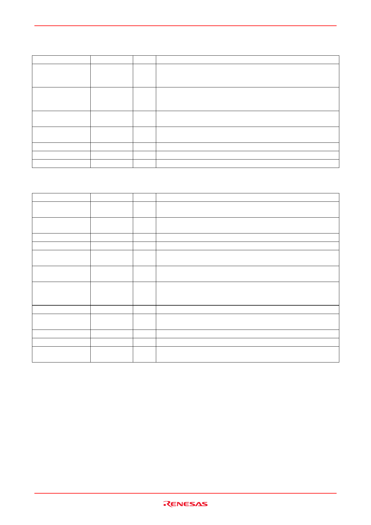
Pin Description
• Common: 13 pins
Pin Name
Symbol
Clock input
CLK
Phase L
PHSL
PLL through
Frequency select
WDQS [4:0]
RDQS
Reset L
P_THROUGH
F_SEL
WDQS
RDQS
RSTL
I/O
I
I
I
I
I
O-Tri
I
Function
CAM Clock. All input signals except OP and DQ reference to rising
edge of CLK. Activates all output signals except IND, LW and GW in
order to control.
Asserted in half operating frequency range. This signal and CLK
generate internal CAM_CLK providing Cycle-A and Cycle-B. Please
refer to another section for details.
Bypasses the PLL circuit. Refer to the Block Diagram.
Setting “L” operates PLL.
Specifies PLL Lock Range depending on CLK operation frequency.
Refer to the Table 1.
Source Synchronous Clock for input signals from OP and DQ.
Source Synchronous Clock for output signals from IND, LW and GW.
Hardware reset for MARIE-Blade.
• Network Processor/ASIC Interface: 110 pins
Pin Name
Symbol
I/O
Function
Chip select
C_SEL
I Enables only chips with High. This signal must be asserted during two
cycles, Cycle-A and Cycle-B.
Operation enable
OP_ENA
I Indicates that commands from OP are valid. This signal must be set
during two cycles, Cycle-A and Cycle-B.
Mode select
MDS
I Selects Normal or Parallel for search, and Normal or Greedy for write.
Op.code [6:0]
OP[6:0]
I OP [6:0] controls command codes. Should be asserted at Cycle-A
DX [3:0]
DX[3:0]
I/O-Tri Extended Data Primary search key is input/output when DX Test
Logic Read/Write/Search command is loaded.
DQ/address [71:0] DQ[71:0]
I/O-Tri Data Pin Multiplexed pin between address and data, which functions
during DQ array Read/Write/Search command.
Index address [17:0] IND[17:0]
O-Tri Input address into externally located SRAMs. Entry address carried by
this pin is search hit address. If ASR is used as write address source,
IND retrieves write address from it.
Local winner flag
LW
O Goes high when search results in hit.
Global winner flag GW
O-Tri Directly outputs prioritized device ID set by ST [9:8] when search
[1:0]
results in hit.
Read data valid
RD_VD
O Qualifies read data when DQ/DX output.
Index valid
IND_VD
O Qualifies read data when IND outputs regardless of search result.
Error check flag
EC_F
O Goes high when Party Bit Check finds any errors. Enable only during a
Read TCAM, whose setting allows error check.
Rev.1.00 Feb 21, 2005 page 8 of 14
Share Link: 