RJP4301APP データシートの表示(PDF) - Renesas Electronics
部品番号
コンポーネント説明
メーカー
RJP4301APP Datasheet PDF : 7 Pages
| |||
RJP4301APP
Electrical Characteristics
Parameter
Collector-emitter breakdown voltage
Collector-emitter leakage current
Gate-emitter leakage current
Gate-emitter threshold voltage
Collector-emitter saturation voltage
Input capacitance
Output capacitance
Reverse transfer capacitance
Turn-on delay time
Rise time
Turn-off delay time
Fall time
Symbol
V(BR)CES
ICES
IGES
VGE(th)
VCE(sat)
Cies
Coes
Cres
td(on)
tr
td(off)
tf
Min.
430
—
—
3.0
—
—
—
—
—
—
—
—
Typ.
—
—
—
—
4.0
1150
125
14
0.01
0.06
0.15
0.2
Max.
—
1
±0.1
5.5
10
—
—
—
—
—
—
—
Unit
V
μA
μA
V
V
pF
pF
pF
μs
μs
μs
μs
(Tj = 25°C)
Test conditions
IC = 100 μA, VGE = 0 V
VCE = 430 V, VGE = 0 V
VGE = ±33 V, VCE = 0 V
VCE = 10 V, IC = 1 mA
IC = 200 A, VGE = 26 V
VCE = 25 V
VGS = 0
f = 1 MHz
ID = 200 A
VGS = 26 V
VCC = 300 V
RG = 25 Ω
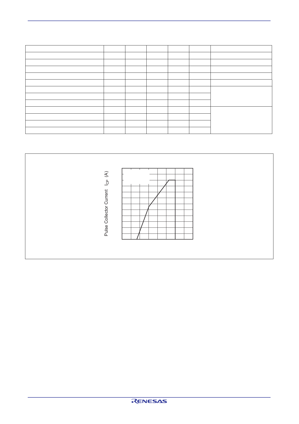
Performance Curves
Maximum Pulse Collector Current
240
CM = 1500 μF
Tc ≤ 70°C
200 RG = 30 Ω
160
120
80
40
0
0
10
20
30
40
Gate-Emitter Voltage VGE (V)
REJ03G1709-0300 Rev.3.00 Oct 14, 2009
Page 2 of 4
Share Link: 