SC4602A データシートの表示(PDF) - Semtech Corporation
部品番号
コンポーネント説明
メーカー
SC4602A Datasheet PDF : 18 Pages
| |||
SC4602A/B
POWER MANAGEMENT
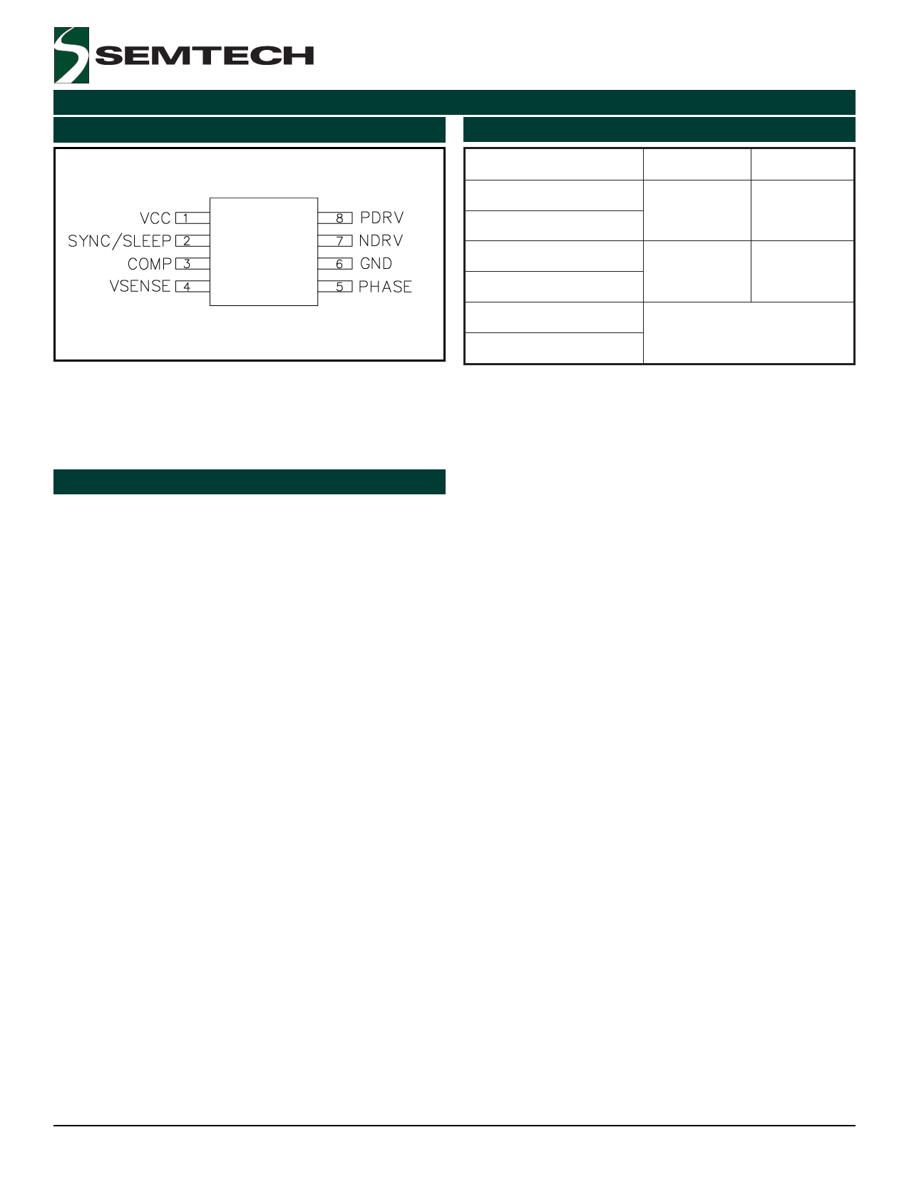
Pin Configuration
Ordering Information
Top View
(8 Pin MSOP)
Part Number(1)
SC4602AIMSTR
SC4602AIMSTRT(2)
SC4602BIMSTR
SC4602BIMSTRT(2)
SC4602AEVB
SC4602BEVB
kHz
Device
300
MSOP-8
550
MSOP-8
Evaluation Board
Pin Descriptions
VCC: Positive supply rail for the IC. Bypass this pin to
GND with a 0.1 to 4.7µF low ESL/ESR ceramic capaci-
tor.
GND: All voltages are measured with respect to this pin.
All bypass and timing capacitors connected to GND should
have leads as short and direct as possible.
SYNC/SLEEP: The oscillator of SC4602A and SC4602B
are set to 300kHz and 550kHz respectively when SYNC/
SLEEP is pulled and held above 2V. Synchronous mode
operation is activated as the SYNC/SLEEP is driven by an
external clock. The oscillator and PWM are designed to
provide practical operation to 450kHz for SC4602A and
to 700kHz for SC4602B when synchronized. Sleep mode
is invoked if SYNC/SLEEP is pulled and held below 0.8V
which can be accomplished by an external gate or tran-
sistor. Sleepmode supply current is 10µA typical.
VSENSE: This pin is the inverting input of the voltage
amplifier and serves as the output voltage feedback point
for the Buck converter. It senses the output voltage through
an external divider.
Notes:
(1) Only available in tape and reel packaging. A reel
contains 2500 devices.
(2) Lead free product. This product is fully WEEE and
RoHS compliant.
PHASE: This input is connected to the junction between
the two external power MOSFET transistors. The voltage
drop across the upper P-channel device is monitored by
PHASE during conduction and forms the current limit
comparator. Logic sets the PWM latch and terminates
the output pulse. The controller stops switching and goes
through a soft start sequence once the converter out-
put voltage drops below 68.75% its nominal voltage. This
prevents excess power dissipation in the PMOSFET dur-
ing a short circuit. The reverse current comparator senses
the drop across the lower N-channel MOSFET during its
conduction and disables the drive signal if a small posi-
tive voltage is present. To disable the overcurrent com-
parator, connect PHASE to VCC.
PDRV, NDRV: The PWM circuitry provides complemen-
tary drive signals to the output stages. Cross conduc-
tion of the external MOSFETS is prevented by monitoring
the voltage on the P-channel and N-channel driver pins
in conjunction with a time delay optimized for FET turn-
off characteristics.
COMP: This is the output of the voltage amplifier. The
voltage at this output is inverted internally and connected
to the non-inverting input of the PWM comparator. A lead-
lag network around the voltage amplifier compensates for
the two pole LC filter characteristic inherent to voltage mode
control and is required in order to optimize the dynamic
performance of the voltage mode control loop.
2006 Semtech Corp.
5
www.semtech.com
Share Link: 