28F016XS データシートの表示(PDF) - Intel
部品番号
コンポーネント説明
メーカー
28F016XS Datasheet PDF : 54 Pages
| |||
28F016XS FLASH MEMORY
E
The BYTE# pin allows either x8 or x16
read/programs to the 28F016XS. BYTE# at logic
low selects 8-bit mode with address A0 selecting
between low byte and high byte. On the other hand,
BYTE# at logic high enables 16-bit operation with
address A1 becoming the lowest order address and
address A0 is not used (don’t care). A device block
diagram is shown in Figure 1.
The 28F016XS incorporates an Automatic Power
Saving (APS) feature, which substantially reduces
the active current when the device is in static mode
of operation (addresses not switching). In APS
mode, the typical ICC current is 1 mA at 5.0V (3 mA
at 3.3V).
A deep power-down mode of operation is invoked
when the RP# (called PWD# on the 28F008SA) pin
transitions low. This mode brings the device power
consumption to less than 2.0 µA, typically, and
provides additional write protection by acting as a
device reset pin during power transitions. A reset
time of 300 ns (5V VCC) is required from RP#
switching high before latching an address into the
28F016XS. In the deep power-down state, the
WSM is reset (any current operation will abort) and
the CSR, GSR and BSR registers are cleared.
A CMOS standby mode of operation is enabled
when either CE0# or CE1# transitions high and RP#
stays high with all input control pins at CMOS
levels. In this mode, the device typically draws an
ICC standby current of 70 µA at 5V VCC.
The 28F016XS is available in 56-Lead, 1.2 mm
thick, 14 mm x 20 mm TSOP and 1.8 mm thick, 16
mm x 23.7 mm SSOP Type I packages. The form
factor and pinout of these two packages allow for
very high board layout densities.
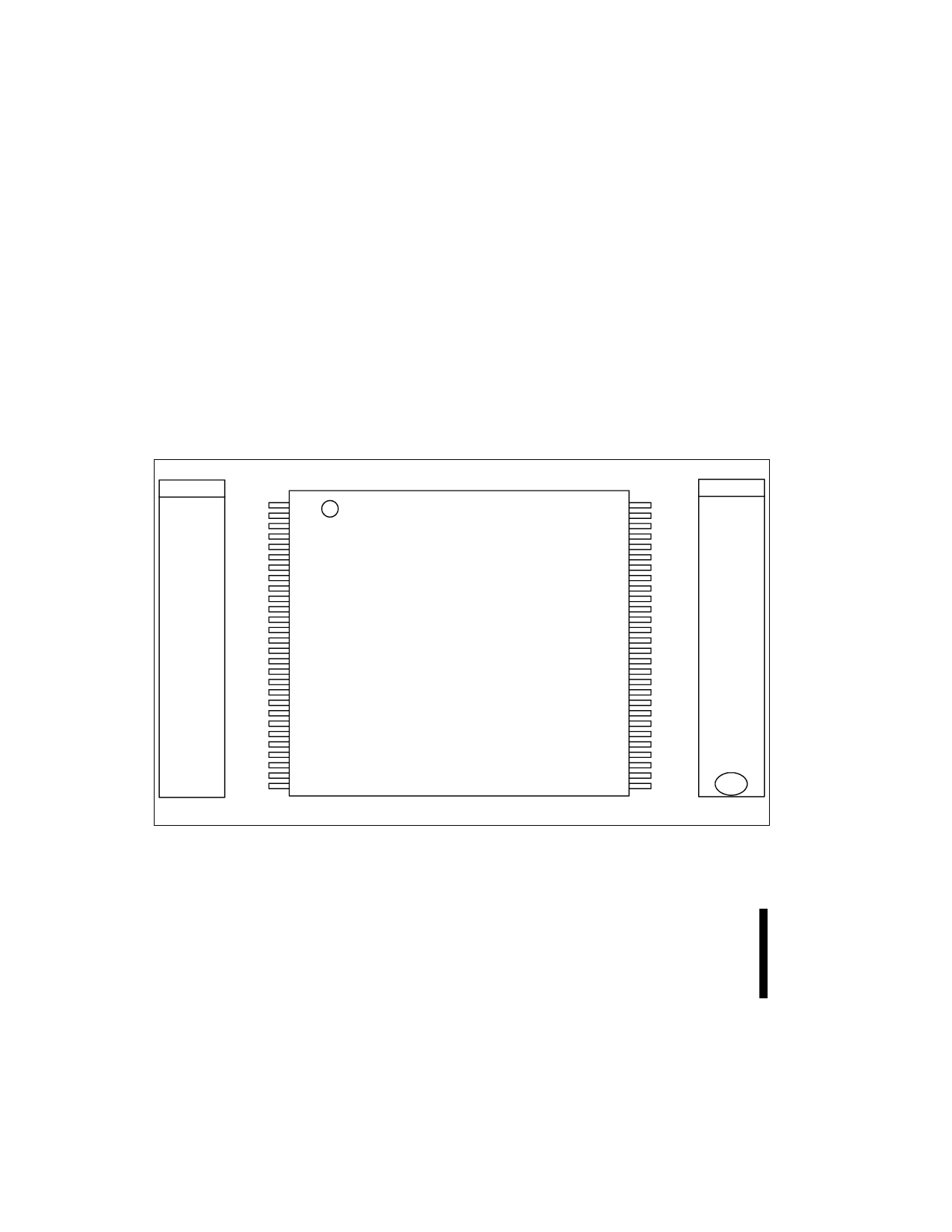
2.0 DEVICE PINOUT
The 28F016XS is pinout compatible with the
28F016SA/SV 16-Mbit FlashFile memory com-
ponents, providing a performance upgrade path to
the 28F016XS. The 28F016XS 56-Lead TSOP and
SSOP pinout configurations are shown in Figures 2
and 3.
28F016SA/SV
3/5#
CE1 #
NC
A 20
A 19
A 18
A 17
A 16
VCC
A 15
A 14
A 13
A 12
CE0 #
VPP
RP#
A 11
A 10
A9
A8
GND
A7
A6
A5
A4
A3
A2
A1
3/5#
1
CE1 #
2
NC
3
A 20
4
A 19
5
A 18
6
A 17
7
A 16
8
V CC
9
A 15
10
A 14
11
A 13
12
A 12
13
CE0 #
14
VPP
15
RP#
16
A 11
17
A 10
18
A9
19
A8
20
GND
21
A7
22
A6
23
A5
A4
24
25
A3
26
A2
27
A1
28
E28F016XS
56-LEAD TSOP PINOUT
14 mm x 20 mm
TOP VIEW
28F016SA/SV
56
WP#
WP#
55
WE#
WE#
54
OE#
OE#
53
RY/BY#
RY/BY#
52
DQ15
51
DQ7
50
DQ14
49
DQ6
48
GND
DQ15
DQ7
DQ14
DQ6
GND
47
DQ 13
46
DQ5
45
DQ12
44
43
DQ4
VCC
DQ13
DQ5
DQ12
DQ4
VCC
42
GND
GND
41
DQ11
40
DQ 3
39
DQ 10
38
DQ 2
DQ11
DQ 3
DQ 10
DQ 2
37
VCC
36
DQ 9
35
DQ 1
34
DQ 8
33
DQ 0
32
A0
31
BYTE#
VCC
DQ9
DQ1
DQ8
DQ0
A0
BYTE#
30
ADV#
NC
29
CLK
NC
0532_02
Figure 2. 28F016XS 56-Lead TSOP Pinout Configuration Shows Compatibility with
the 28F016SA/SV, Allowing for Easy Performance Upgrades from Existing 16-Mbit Designs
10
Share Link: 