TC530CKW データシートの表示(PDF) - TelCom Semiconductor, Inc
部品番号
コンポーネント説明
メーカー
TC530CKW Datasheet PDF : 15 Pages
| |||
5V PRECISION DATA ACQUISITION
SUBSYSTEMS
1
TC530
TC534
PIN DESCRIPTION (Cont.)
Pin No. Pin No. Pin No Pin No.
2
(TC530 (TC530 (TC534 (TC534
28-Pin
28-Pin 40-Pin 44-Pin
PDIP, 300 Mil.) SOIC) PDIP) PQFP) Symbol Description
22
23
25
26
27
28
13, 24
22
32
30
VCCD Analog Input. Power supply connection for digital logic and
serial port. Proper power-up sequencing is critical, see the
Applications section.
23
34
32
OSC
Input. The negative power supply converter normally runs at
a frequency of 100kHz. This frequency can be slowed down to
3
reduce quiescent current by connecting an external capacitor
between this pin and VS+. (See Typical Characteristics).
25
37
35
VDD
Analog Input. Power supply connection for the A/D analog
section and DC-DC converter. Proper power-up sequencing is
critical, see the Applications section.
26
38
27
39
28
40
36
CAP+ Analog Input. Storage capacitor positive connection for the
DC/DC converter.
37
AGND Analog Input. Ground connection for DC/DC converter.
4
38
CAP– Analog Input. Storage capacitor negative connection for the
DC/DC converter.
13, 24 28, 29, 31, 1, 25, 26, 27 NC
33, 35, 36 29, 31, 33,
34, 39, 44,
No connect. Do not connect any signal to these pins.
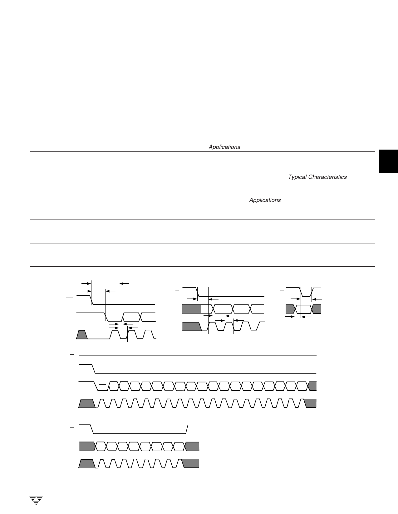
R/W
EOC
DOUT
DCLK
R/W
READ TIMING
tRS
tRD
tDRS
tPWL
R/W
DIN
DCLK
WRITE TIMING
tLS
tDLS tPWL
READ FORMAT
WRITE DEFAULT TIMING
R/W
DIN
tLDL
tLDS
5
6
EOC
DOUT
EOC OVR SGN MSB
LSB
DCLK
R/W
WRITE FORMAT
7
DOUT
MSB
LSB
DCLK
For Polled vs Interrupt Operation and Write Value Modified Cycle Use TC520A Data Sheet Figure 1 & 2.
Figure 1. Serial Port Timing
TELCOM SEMICONDUCTOR, INC.
8
3-53
Share Link: 