TC534CPL データシートの表示(PDF) - TelCom Semiconductor, Inc
部品番号
コンポーネント説明
メーカー
TC534CPL Datasheet PDF : 15 Pages
| |||
TC530
TC534
5V PRECISION DATA ACQUISITION
SUBSYSTEMS
Conversion
Phase
AZ
INT
Data to Serial
Port Transmit
Register
EOC
Updated Data
Ready
tDR
DINT
IZ
AZ
Updated Data
Ready
Figure 2. A/D Converter Timing
DETAILED DESCRIPTION
Dual Slope Integrating Converter
The TC530/534 dual slope converter operates by inte-
grating the input signal for a fixed time period, then applying
an opposite polarity reference voltage while timing the
period (counting clocks pulses) for the integrator output to
cross 0V (deintegrating). The resulting count is read as
conversion data.
A simple mathematical expression that describes dual
slope conversion is:
(1) Integrate Voltage = Deintegrate Voltage
∫ ∫ (2) 1/RINTCINT
tINT
VIN(t)dt = 1/RINTCINT
0
tDINT
VREF
0
from which:
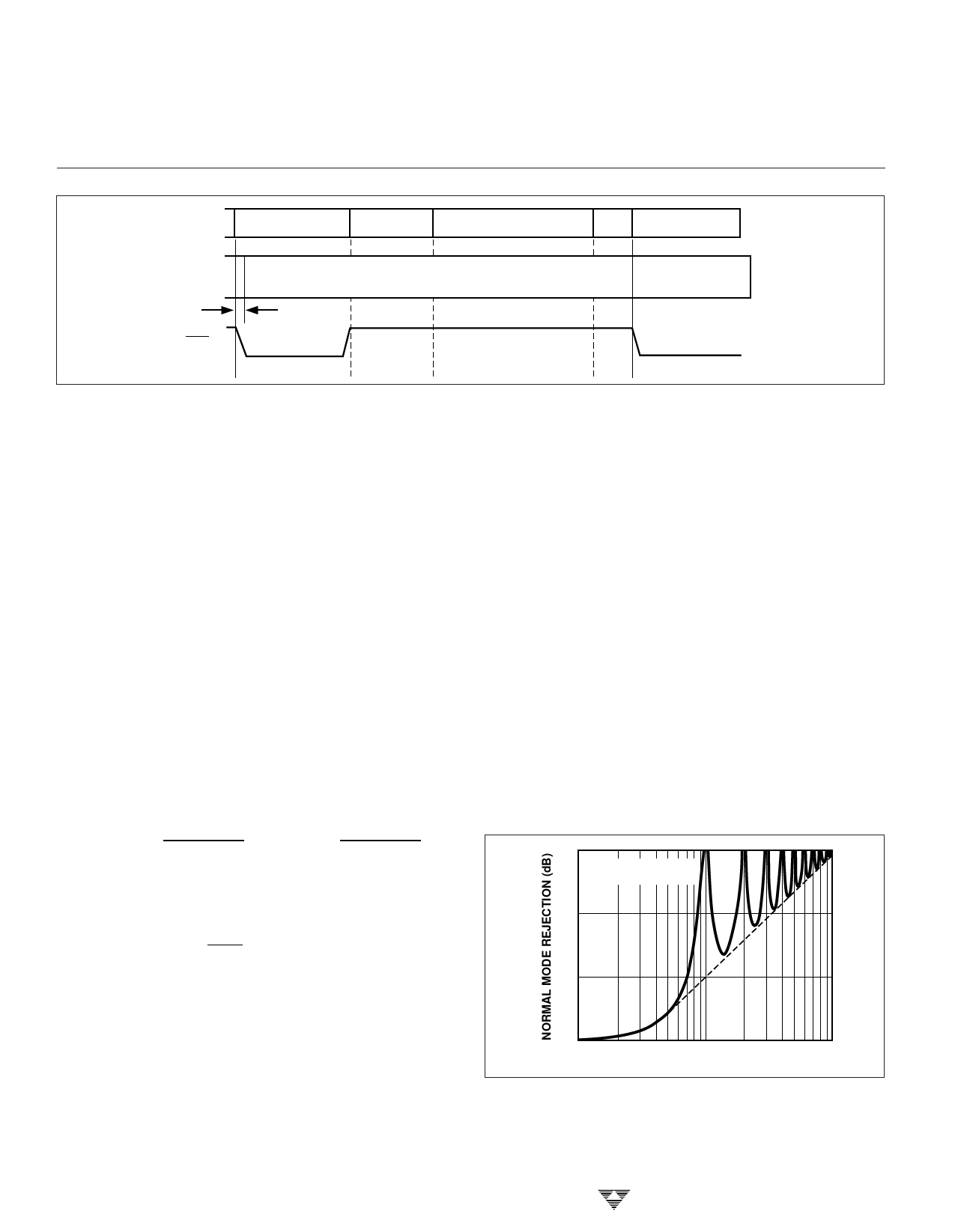
Another inherent benefit is noise immunity. Input noise
spikes are integrated (or averaged to zero) during the
integration period. The integrating converter has a noise
immunity with an attenuation rate of at least –20dB per
decade. Interference signals with frequencies at integral
multiples of the integration period are, for the most part,
completely removed. For this reason, the integration period
of the converter is often established to reject 50/60Hz line
noise. The ability to reject such noise is shown by the plot of
Figure 3.
In addition to the two phases required for dual slope
measurement (Integrate and Deintegrate), the TC530/534
performs two additional adjustments to minimize measure-
ment error due to system offset voltages. The resulting four
internal operations (conversion phases) performed each
measurement cycle are: Auto Zero (AZ), Integrator Output
Zero (IZ), Input Integrate (INT) and Reference Deintegrate
(DINT). The AZ and IZ phases compensate for system offset
errors and the INT and DINT phases perform the actual A/D
conversion.
[ ] [ ] (3) (VIN)
(tINT)
(RINT)(CINT)
= (VREF)
(tDINT)
(RINT)(CINT)
and therefore:
[ ] (4) VIN = VREF
tDINT
tINT
where: VREF = Reference Voltage
tINT = Integrate Time
tDINT = Reference Voltage Deintegrate Time
Inspection of equation (4) shows dual slope converter
accuracy is unrelated to integrating resistor and capacitor
values, as long as they are stable throughout the measure-
ment cycle. This measurement technique is inherently
ratiometric (i.e., the ratio between the tINT and tDINT times is
equal to the ratio between VIN and VREF).
3-54
30
T = MEASUREMENT
PERIOD
20
10
0
0.1/T
1/T
INPUT FREQUENCY
10/T
Figure 3. Integrating Converter Normal Mode Rejection
TELCOM SEMICONDUCTOR, INC.
Share Link: 