TC660COA データシートの表示(PDF) - TelCom Semiconductor, Inc
部品番号
コンポーネント説明
メーカー
TC660COA Datasheet PDF : 8 Pages
| |||
100mA CHARGE PUMP DC-TO-DC
VOLTAGE CONVERTER
TC660
1
8
2
7
3 TC660 6
4
5
V+
D1
VOUT =
D2
(2 V+) – (2 VF)
+
C1
+
C2
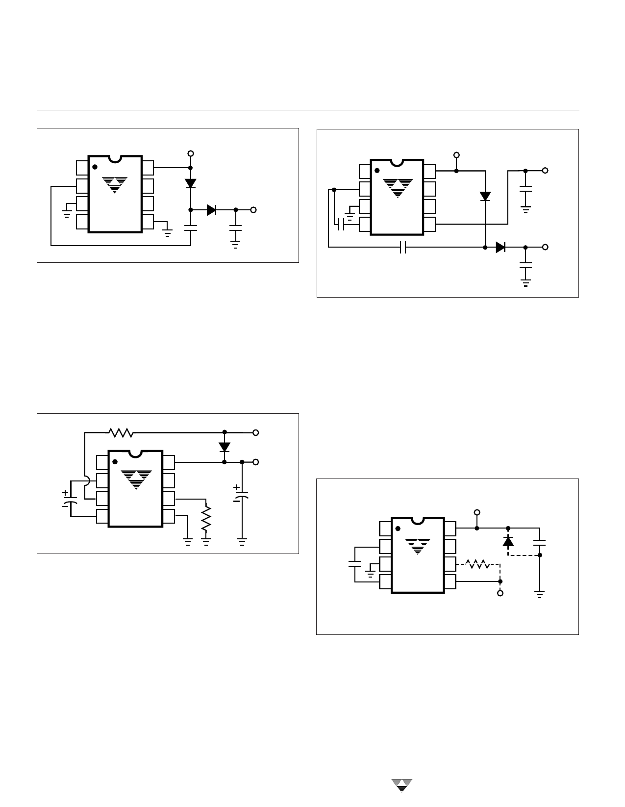
Figure 8. Positive Voltage Doubler
Figure 9 shows an improved way of using the TC660 as
a voltage doubler.
In this circuit, C1 is first charged to VIN and C2 is quickly
brought to within a diode drop of VIN (to prevent substrate
reversal) through D. The optional 200 Ω resistor is only to
limit the brief latchup current.
On the next half-cycle, VIN is in series with C1; C2 is then
charged to 2 VIN. D is now reverse-biased and plays no
further part. For VIN < 3V, R may be necessary to ensure
startup.
200
1
8
2
7
C1
3 TC660 6
4
5
R = 0.1 – 1MΩ
VIN
D
VOUT
= 2 VIN
C2
R
Figure 9. Improved Voltage Doubler
Combined Negative Voltage Conversion
and Positive Supply Multiplication
Figure 10 combines the functions shown in Figures 3
and 8 to provide negative voltage conversion and positive
voltage multiplication simultaneously. In this instance, ca-
pacitors C1 and C3 perform the pump and reservoir func-
tions, respectively, for the generation of the negative volt-
age, while capacitors C2 and C4 are pump and reservoir,
respectively, for the multiplied positive voltage. There is a
penalty in this configuration in that the source impedances
of the generated supplies will be somewhat higher due to
the finite impedance of the common charge pump driver at
pin 2 of the device.
V+
1
8
2
7
3 TC660 6
+
4
C1
5
+
C2
VOUT = –V+
D1
+ C3
D2
V(2OVU+T)
=
–
(2
VF)
+
C4
Figure 10. Combined Negative Converter and Positive Multiplier
Efficient Positive Voltage
Multiplication/Conversion
Since the switches that allow the charge pumping op-
eration are bidirectional, the charge transfer can be per-
formed backward as easily as forward. Figure 11 shows a
TC660 transforming –5V to +5V. The only problem here is
that the internal clock and switch-drive section will not
operate until some positive voltage has been generated. A
diode and resistor shown dotted in Figure 11 can be used to
"force" the internal regulator on.
C1 +
150 µF
VOUT = –V–
1
8
2
7
1 MΩ
3 TC660 6
+
150 µF
4
5
V– INPUT
Figure 11. Positive Voltage Multiplier
4-12
TELCOM SEMICONDUCTOR, INC.
Share Link: 