QT140 データシートの表示(PDF) - Quantum Research Group
部品番号
コンポーネント説明
メーカー
QT140 Datasheet PDF : 14 Pages
| |||
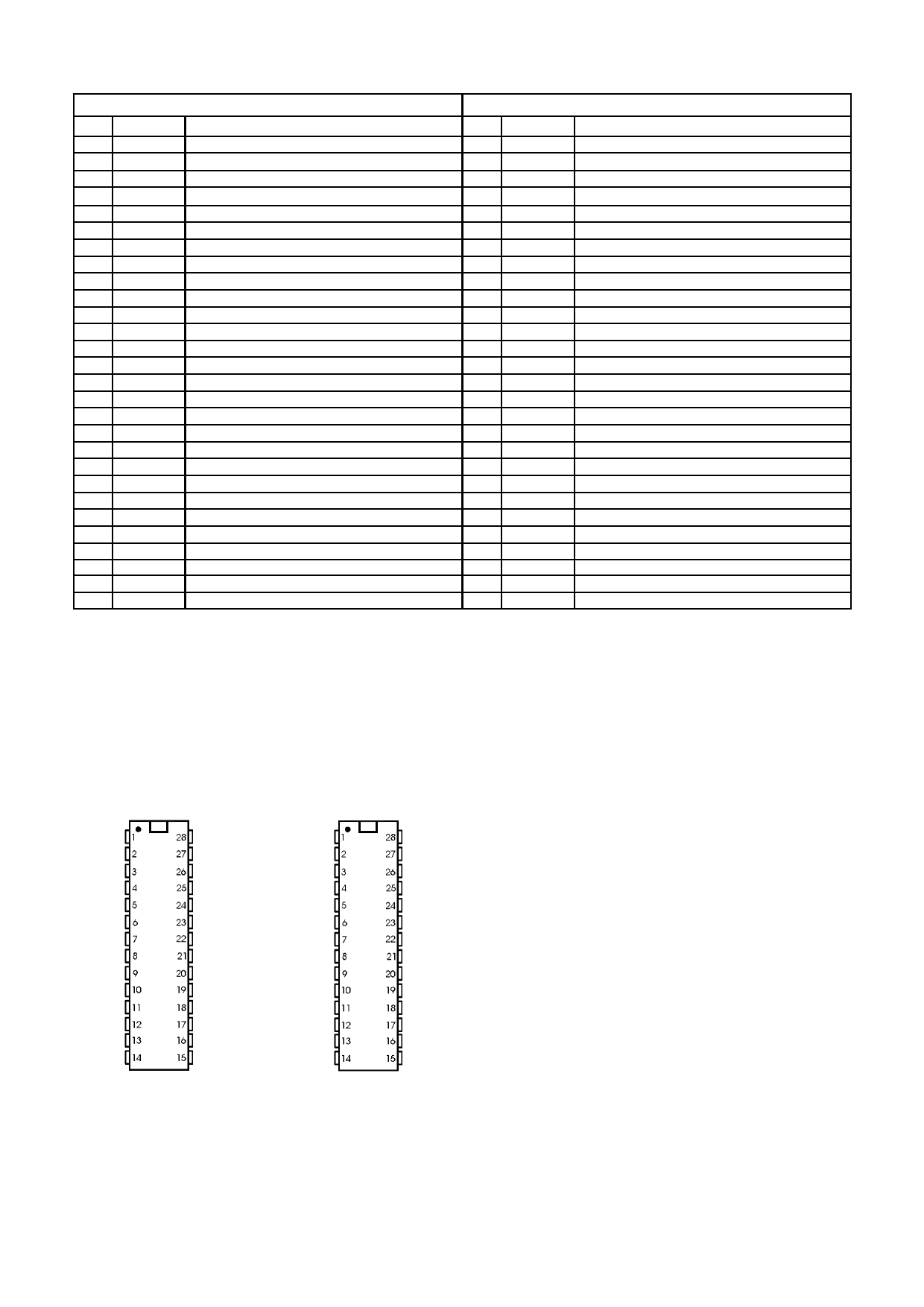
Table 1-1 Pin Listing
QT140 / QT150 SSOP-28
Pin Name Description
1 Vss
Negative power (Ground)
2 Vss
Negative power (Ground)
3 Vdd
Positive power
4 Vdd
Positive power
5 SNS1A
Sense pin (to Cs1, electrode)
6 SNS1B
Sense pin (to Cs1)
7 SNS2A
Sense pin (to Cs2, electrode)
8 SNS2B
Sense pin (to Cs2)
9 SNS3A
Sense pin (to Cs3, electrode)
10 SNS3B
Sense pin (to Cs3)
11 SNS4A
Sense pin (to Cs4, electrode)
12 SNS4B
Sense pin (to Cs4)
13 NC/SNS5A Sense pin (to Cs5, electrode) n/c on QT140
14 Vss
Supply negative rail (ground)
15 NC/SNS5B Sense pin (to Cs5) n/c on QT140
16 OC
Output Option (input pin; 1= open drain)
17 AKS
Adjacent Key Suppression Opt. (input; 1=AKS)
18 OUT1
Channel 1 output, o-d or p-p
19 OUT2
Channel 2 output, o-d or p-p
20 OUT3
Channel 3 output, o-d or p-p
21 OUT4
Channel 4 output, o-d or p-p
22 NC/OUT5 Channel 5 output, o-d or p-p (n/c on QT140)
23 SYNC
Synchronization pin (I/O pin - pull high with 10K)
24 OPT1
Option Mode (Input pin - see Table 2-1)
25 OPT2
Option Mode (Input pin - see Table 2-1)
26 OSC_O
27 OSC_I
Oscillator output
Oscillator input
28 /RST
Reset pin (active low input)
QT140 / QT150 DIP-28
Pin Name Description
1 Vdd
Positive power
2 Vdd
Positive power
3 Vss
Negative power (Ground)
4 Vss
Negative power (Ground)
5 Vss
Negative power (Ground)
6 SNS1A
Sense pin (to Cs1, electrode)
7 SNS1B
Sense pin (to Cs1)
8 SNS2A
Sense pin (to Cs2, electrode)
9 SNS2B
Sense pin (to Cs2)
10 SNS3A
Sense pin (to Cs3, electrode)
11 SNS3B
Sense pin (to Cs3)
12 SNS4A
Sense pin (to Cs4, electrode)
13 SNS4B
Sense pin (to Cs4)
14 NC/SNS5A Sense pin (to Cs5, electrode) n/c on QT140
15 NC/SNS5B Sense pin (to Cs5) n/c on QT140
16 OC
Output Option (input pin; 1= open drain)
17 AKS
Adjacent Key Suppression Opt. (input ; 1=AKS)
18 OUT1
Channel 1 output, o-d or p-p
19 OUT2
Channel 2 output, o-d or p-p
20 OUT3
Channel 3 output, o-d or p-p
21 OUT4
Channel 4 output, o-d or p-p
22 NC/OUT5 Channel 5 output, o-d or p-p (n/c on QT140)
23 SYNC
Synchronization pin (I/O pin - pull high with 10K)
24 OPT1
Option Mode (Input pin - see Table 2-1)
25 OPT2
Option Mode (Input pin - see Table 2-1)
26 OSC_O
27 OSC_I
Oscillator output
Oscillator input
28 /RST
Reset pin (active low input)
1 - OVERVIEW
QT140/150 devices are burst mode digital charge-transfer
(QT) sensor ICs designed specifically for touch controls; they
include all hardware and signal processing functions
necessary to provide stable sensing under a wide variety of
conditions. Only a single low cost capacitor per channel is
required for operation.
Figures 1-6 and 1-7 show basic circuits for these devices.
See Table 1-1 for device pin listings.
Vss
Vss
Vdd
Vdd
SNS1A
SNS1B
SNS2A
SNS2B
SNS3A
SNS3B
SNS4A
SNS4B
NC
Vss
SSOP
/RST
OSC_I
OSC_O
OPT2
OPT1
SYNC
NC
OUT4
OUT3
OUT2
OUT1
AKS
OC
NC
DIP
Vdd
Vdd
Vss
Vss
Vss
SNS1A
SNS1B
SNS2A
SNS2B
SNS3A
SNS3B
SNS4A
SNS4B
NC
/RST
OSC_I
OSC_O
OPT2
OPT1
SYNC
NC
OUT4
OUT3
OUT2
OUT1
AKS
OC
NC
Fig 1-1 QT140 Pinouts
NOTE: SSOP / DIP Pinouts are not the same!
The DIP and SOIC pinouts are not the same and serious
damage can occur if a part is miswired.
1.1 BASIC OPERATION
The devices employ bursts of charge-transfer cycles to
acquire signals. Burst mode permits low power operation,
dramatically reduces RF emissions, lowers susceptibility to
RF fields, and yet permits excellent speed. Internally, signals
are digitally processed to reject impulse noise using a
'consensus' filter that requires three consecutive
confirmations of detection. Each channel is measured in
sequence starting with Channel 1.
The QT switches and charge measurement hardware
functions are all internal to the device. A single-slope
switched capacitor ADC includes the QT charge and transfer
switches in a configuration that provides direct ADC
conversion; an external Cs capacitor accumulates the charge
from sense-plate Cx, which is then measured.
Larger values of Cx cause the charge transferred into Cs to
rise more rapidly, reducing available resolution; as a
minimum resolution is required for proper operation, this can
result in dramatically reduced gain. Conversely, larger values
of Cs reduce the rise of differential voltage across it,
increasing available resolution by permitting longer QT
bursts. The value of Cs can thus be increased to allow larger
values of Cx to be tolerated. The IC is responsive to both Cx
and Cs, and changes in Cs can result in substantial changes
in sensor gain.
lQ
2
QT140/150 1.01/1102
Share Link: 