MAX3042BCSE „Éá„Éľ„āŅ„ā∑„Éľ„Éą„ĀģŤ°®Á§ļÔľąPDFÔľČ - Maxim Integrated
ťÉ®ŚďĀÁē™ŚŹ∑
„ā≥„É≥„ÉĚ„Éľ„Éć„É≥„ÉąŤ™¨śėé
„É°„Éľ„āę„Éľ
MAX3042BCSE Datasheet PDF : 15 Pages
| |||
¬Ī10kV ESD-Protected, Quad 5V RS-485/RS-422
Transmitters
ABSOLUTE MAXIMUM RATINGS
All voltages referenced to ground (GND).
Supply Voltage (VCC).............................................................+7V
Control Input Voltage (EN, EN, EN_) .........-0.3V to (VCC + 0.3V)
Driver Input Voltage (T_IN).........................-0.3V to (VCC + 0.3V)
Driver Output Voltage (Y_, Z_)
(Driver Disabled) .............................................-7.5V to +12.5V
Driver Output Voltage (Y_, Z_)
(Driver Enabled) .................................................-7.5V to +10V
Continuous Power Dissipation (TA = +70¬įC)
16-Pin TSSOP (derate 9.4mW/¬įC above +70¬įC) ..........755mW
16-Pin Narrow SO (derate 8.70mW/¬įC above +70¬įC) ..696mW
16-Pin Wide SO (derate 9.52mW/¬įC above +70¬įC) .....762mW
Operating Temperature Range
MAX304_C_E .......................................................0¬įC to +70¬įC
MAX304_E_E ....................................................-40¬įC to +85¬įC
Maximum Junction Temperature .....................................+150¬įC
Storage Temperature Range .............................-65¬įC to +150¬įC
Lead Temperature (soldering, 10s) .................................+300¬įC
Stresses beyond those listed under ‚ÄúAbsolute Maximum Ratings‚ÄĚ may cause permanent damage to the device. These are stress ratings only, and functional
operation of the device at these or any other conditions beyond those indicated in the operational sections of the specifications is not implied. Exposure to
absolute maximum rating conditions for extended periods may affect device reliability.
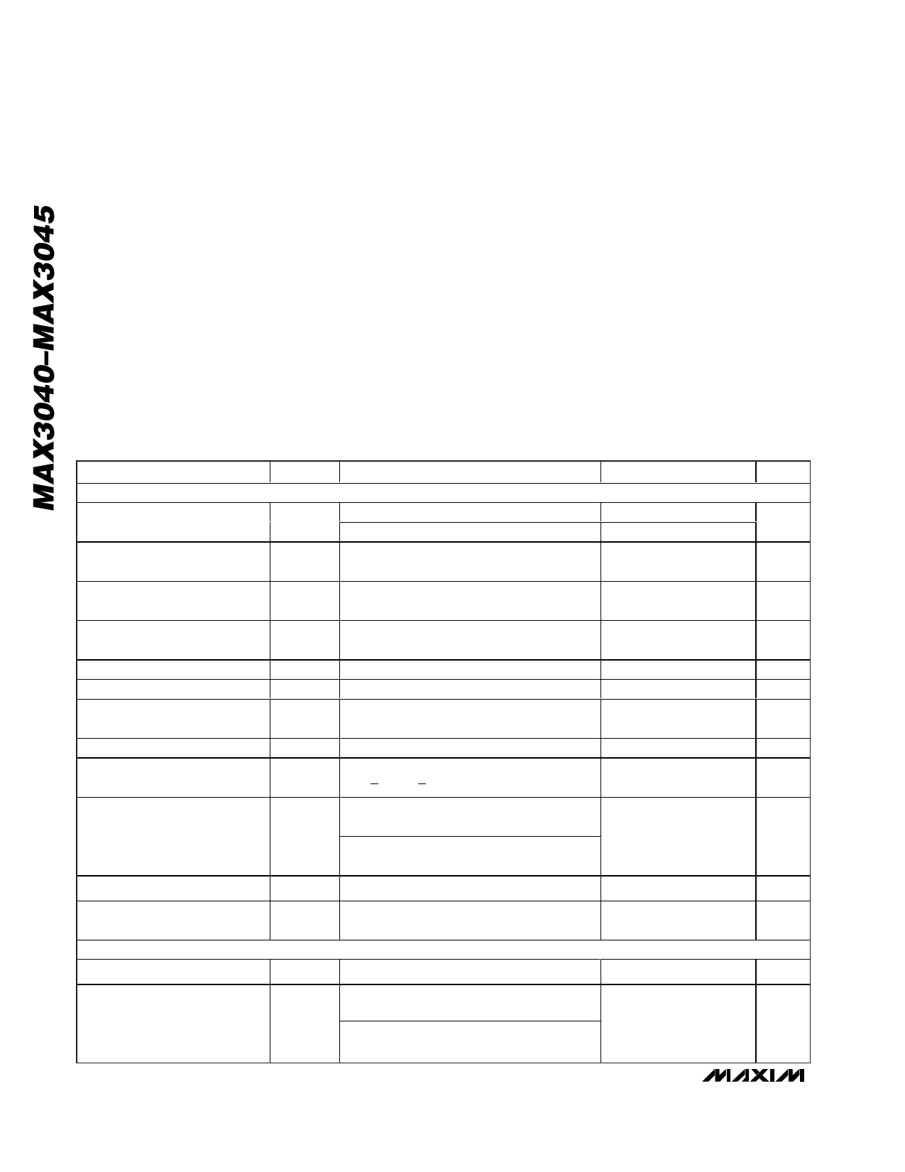
ELECTRICAL CHARACTERISTICS
(VCC = +5V ¬Ī5%, TA = TMIN to TMAX, unless otherwise noted. Typical values are at VCC = +5V and TA = +25¬įC.) (Note 1)
PARAMETER
DRIVER
Driver Differential Output
SYMBOL
CONDITIONS
Figure 1, R = 50‚Ą¶
VOD
Figure 1, R = 27‚Ą¶
MIN TYP MAX UNITS
2.0
V
1.5
Change in Magnitude of
Differential Output Voltage
‚ąÜVOD Figure 1, R = 50‚Ą¶ or 27‚Ą¶ (Note 2)
0.2
V
Driver Common-Mode Output
Voltage
VOC
Figure 1, R = 50‚Ą¶ or 27‚Ą¶
VCC / 2 3
V
Change In Magnitude of
Common-Mode Voltage
‚ąÜVOC Figure 1, R = 50‚Ą¶ or 27‚Ą¶ (Note 2)
0.2
V
Input High Voltage
Input Low Voltage
VIH
T_IN, EN_, EN, EN
VIL
T_IN, EN_, EN, EN
2.0
V
0.8
V
Hot-Swap Driver Input Current
IHOT
SWAP
EN_, EN, EN (Note 3)
¬Ī200
¬ĶA
Driver Input Current
IIN
T_IN, EN_, EN, EN
¬Ī1
¬ĶA
Driver Short-Circuit Output
Current
ISC
-7V < VOUT < +10V (Note 4)
¬Ī25
¬Ī250
mA
Output Leakage (Y_, Z_)
when Disabled
ESD Protection (Y_, Z_)
MAX3040/MAX3041/MAX3042B
EN_ = GND
MAX3043/MAX3044/MAX3045B
EN = GND, EN = VCC
Human Body Model
¬Ī1
¬ĶA
¬Ī10
kV
Electrical Fast Transient/Burst
Immunity
SUPPLY CURRENT
IEC 1000-4-4
¬Ī4
kV
Supply Current
Supply Current in Shutdown
Mode
ICC
ISHDN
No load
MAX3040/MAX3041/MAX3042B
EN_ = GND, TA = +25¬įC
MAX3043/MAX3044/MAX3045B
EN = GND, EN = VCC, TA = +25¬įC
1
2
mA
0.002 10
¬ĶA
2 _______________________________________________________________________________________
Share Link: 