MAX3042BCSE „Éá„Éľ„āŅ„ā∑„Éľ„Éą„ĀģŤ°®Á§ļÔľąPDFÔľČ - Maxim Integrated
ťÉ®ŚďĀÁē™ŚŹ∑
„ā≥„É≥„ÉĚ„Éľ„Éć„É≥„ÉąŤ™¨śėé
„É°„Éľ„āę„Éľ
MAX3042BCSE Datasheet PDF : 15 Pages
| |||
¬Ī10kV ESD-Protected, Quad 5V RS-485/RS-422
Transmitters
Detailed Description
The MAX3040‚ÄďMAX3045 are quad RS-485/RS-422 trans-
mitters. They operate from a single +5V power supply
and are designed to give optimum performance when
used with the MAX3093E/MAX3095 5V quad RS-485/
RS-422 receivers or MAX3094E/MAX3096 3V quad
RS-485/RS-422 receivers. The MAX3040‚ÄďMAX3045 only
need 1mA of operating supply current and consume 2nA
when they enter a low-power shutdown mode. The
MAX3040‚ÄďMAX3045 also feature a hot-swap capability
allowing line insertion without erroneous data transfer.
The MAX3042B/MAX3045B are capable of transferring
data up to 20Mbps, the MAX3041/MAX3044 for data
rates up to 2.5Mbps, and the MAX3040/MAX3043 for
data rates up to 250kbps. All transmitter outputs are pro-
tected to ¬Ī10kV using the Human Body Model.
¬Ī10kV ESD Protection
As with all Maxim devices, ESD-protection structures
are incorporated on all pins to protect against electro-
static discharges (ESD) encountered during handling
and assembly. The MAX3040‚ÄďMAX3045 transmitter
outputs have extra protection against electrostatic dis-
charges found in normal operation. Maxim’s engineers
have developed state-of-the-art structures to protect
these pins against the application of ¬Ī10kV ESD
(Human Body Model), without damage.
Y
R
VOD
VOC
R
ESD Test Conditions
ESD performance depends on a number of conditions.
Contact Maxim for a reliability report that documents
test setup, methodology, and results.
Human Body Model
Figure 6a shows the Human Body Model, and Figure
6b shows the current waveform it generates when dis-
charged into low impedance. This model consists of a
100pF capacitor charged to the ESD voltage of interest,
which is then discharged into the device through a
1.5k‚Ą¶ resistor.
3V
DI
1.5V
0
tPLH
1.5V
tPHL
1/2 VO
Z
VO
Y
1/2 VO
VDIFF = V (Y) - V (Z)
VDIFF
VO
0
-VO
10%
90%
90%
10%
tR
tF
tSKEW = | tPLH - tPHL |
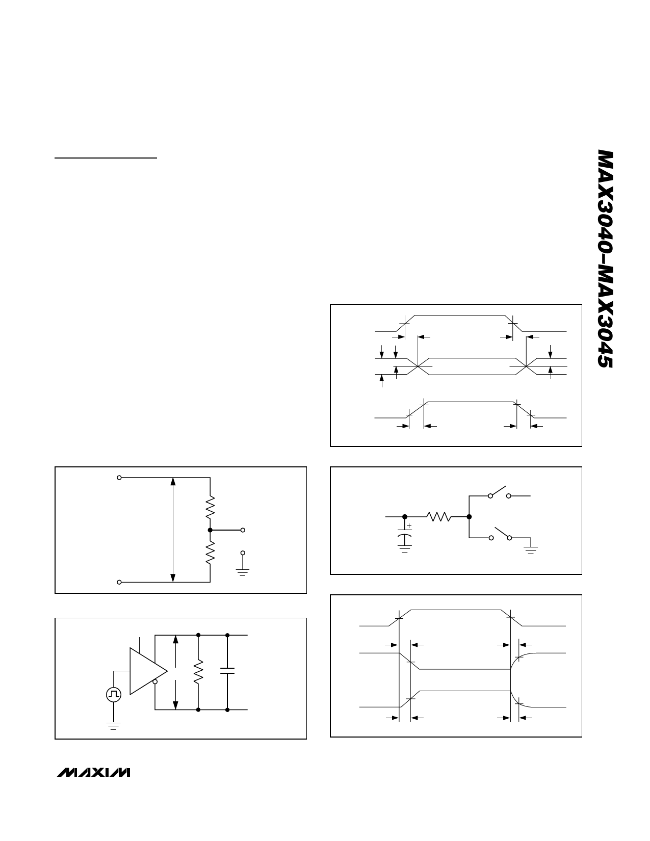
Figure 3. Driver Propagation Delays
OUTPUT
UNDER TEST
RL
CL
VCC
S1
S2
Z
Figure 1. Driver DC Test Circuit
5V
DE
DI
Y
VOD
Z
RDIFF
CDIFF
Figure 4. Driver Enable/Disable Timing Test Load
3V
DE
1.5V
0
Y, Z
VOL
Y, Z
0
1.5V
tZL(SHDN), tZL
tLZ
2.5V OUTPUT NORMALLY LOW
OUTPUT NORMALLY HIGH
2.5V
tZH(SHDN), tZH
tHZ
VOL +0.5V
VOH -0.5V
Figure 2. Driver Timing Test Circuit
Figure 5. Driver Enable and Disable Times
_______________________________________________________________________________________ 7
Share Link: 