NJU6682 データシートの表示(PDF) - Japan Radio Corporation
部品番号
コンポーネント説明
メーカー
NJU6682 Datasheet PDF : 58 Pages
| |||
NJU6682
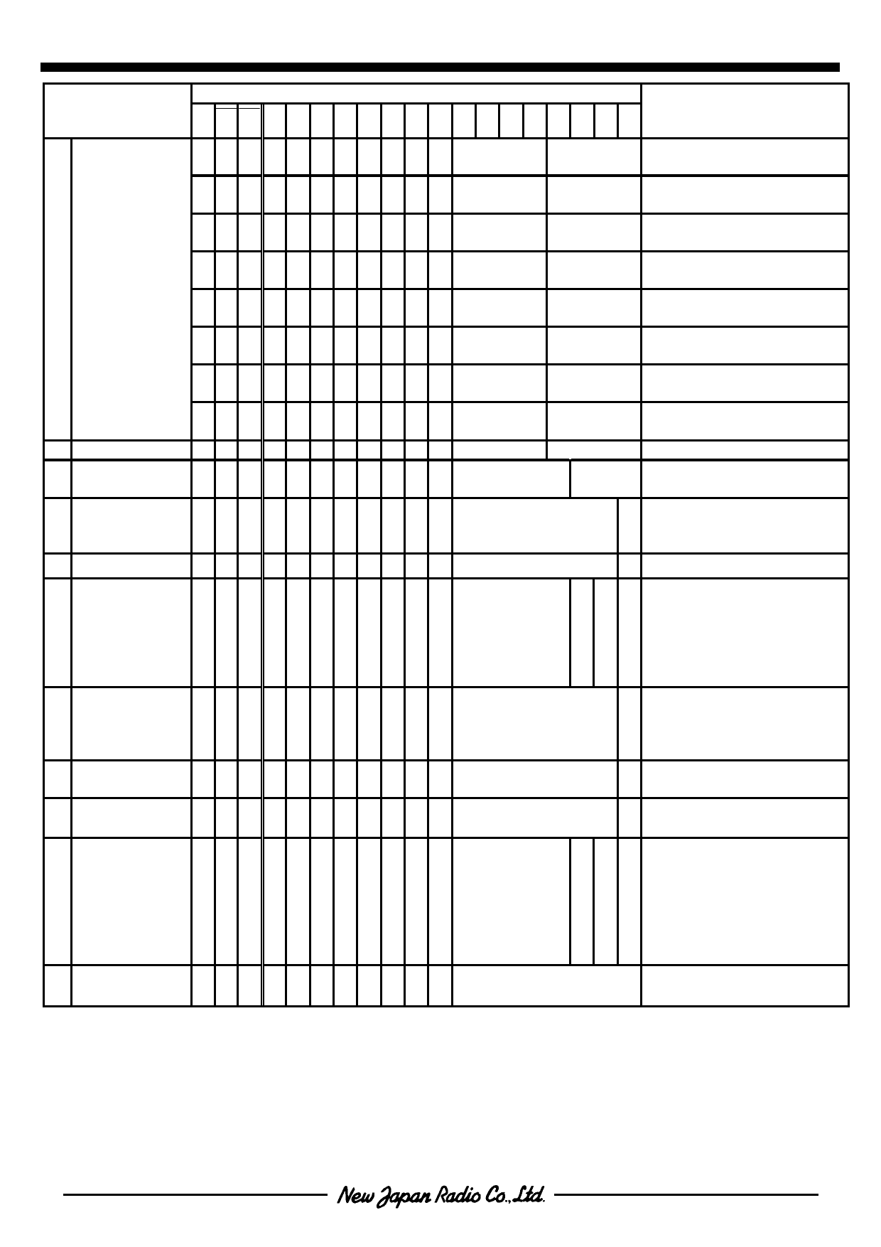
Instruction
Code
A0 RD WR D15 D14 D13 D12 D11 D10 D9 D8 D7 D6 D5 D4 D3 D2 D1 D0
Description
Select
(14)
Gray Scale Level
(15)
Bias Select
Voltage Converter
(16)
Multiple Select
Read Modify Write
(17)
/End
(18)
Reset
Internal
(19)
Power Supply
Driver Outputs
(20)
ON/OFF
Powehr Save
(21)
(dual command)
(22) ADC Select
Display Mode
(23)
Select
8-bit/16-bit
(24)
Bus Select
PWM Data
0 1 0 0 1 1 1 0 0 00
(Frame No.1)
PWM Data
010 01110001
(Frame No.3)
PWM Data
010 01110010
(Frame No.1)
PWM Data
010 01110011
(Frame No.3)
PWM Data
010 01110100
(Frame No.1)
PWM Data
010 01110101
(Frame No.3)
PWM Data
010 01110110
(Frame No.1)
PWM Data
010 01110111
(Frame No.3)
010 00001001
*
010 00001010
*
PWM Data
(Frame No.2)
PWM Data
(Frame No.4)
PWM Data
(Frame No.2)
PWM Data
(Frame No.4)
PWM Data
(Frame No.2)
PWM Data
(Frame No.4)
PWM Data
(Frame No.2)
PWM Data
(Frame No.4)
Bias
Boost
Multiple
Gray Scale Level 0:Set the PWM
Data of Frame No.1 and No.2
Gray Scale Level 0:Set the PWM
Data of Frame No.3 and No.4
Gray Scale Level 1:Set the PWM
Data of Frame No.1 and No.2
Gray Scale Level 1:Set the PWM
Data of Frame No.3 and No.4
Gray Scale Level 2:Set the PWM
Data of Frame No.1 and No.2
Gray Scale Level 2:Set the PWM
Data of Frame No.3 and No.4
Gray Scale Level 3:Set the PWM
Data of Frame No.1 and No.2
Gray Scale Level 3:Set the PWM
Data of Frame No.3 and No.4
Select Bias (11 types)
Set the Boost Multiple :2 to 7 times
010 00010000
*
010 00010001
*
Increase X Address Counter +1 when
0
writing but no-change when reading
1
D0=0:ON D0=1:END
1 Initialize the internal circuits
010 00010010
DC=1:Voltage converter ON
DC=0:Voltage converter OFF
VR=1:Voltage Regurator ON
*
DC VR VF
VR=0:Voltage Regurator OFF
VF=1:Voltage Follower ON
VF=0:Voltage Follower OFF
010 00010011
*
010 00000000
*
010 00000010
Set LCD driver outputs after the inter-
0 nal(external) power supply ON
1 D0=0:Driver Outouts OFF
D0=1:Driver Outputs ON
0 Set the Power Save mode
1 (Reverse input sequence is possible)
010 00011000
*
0 Output the Disp. RAM address Sn
1 D0=0:Normal D0=1:Reverse
010 00011001
0
010 0001101
1
Set Display mode
GB=1:Gray scale mode
GB=0:Black and white mode
*
GS L1 L0 L1=1:Select layer 1
L1=0:Not select layer 1
L0=1:select layer 0
L0=0:Not select layer 0
D8=0:Set 8-bit interface bus
*
D8=1:Set 16-bit interface bus
( * : Don’t care)
Share Link: 