VRE4100 データシートの表示(PDF) - Unspecified
部品番号
コンポーネント説明
メーカー
VRE4100 Datasheet PDF : 7 Pages
| |||
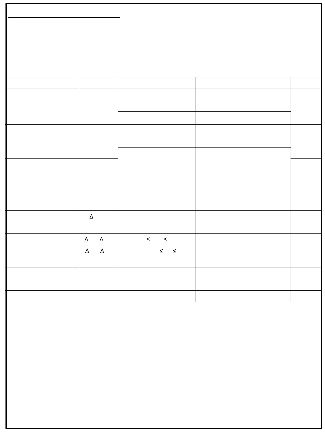
ABSOLUTE MAXIMUM RATINGS
Power supply to any input pin ….…-0.3V to +5.6V
Operating Temp. (B,C) …………..……0°C to 70°C
Operating Temp. (K)………………...-40°C to 85°C
Storage Temperature Range……..-65°C to 150°C
Output Short Circuit Duration …….…………....Indefinite
ESD Susceptibility Human Body Model…….…..…..2kV
ESD Susceptibility Machine Model ..………………200V
Lead Temperature (soldering,10 sec)………...….260°C
ELECTRICAL SPECIFICATIONS
Vps =+3V for VRE4110 and VRE4112, Vps =+5V for VRE4125, VRE4125 and VRE4141. T = 25°C, Iload=1mA, Cout=1µF unless otherwise noted.
PARAMETER
SYMBOL
CONDITIONS
MIN TYP MAX
Input Voltage
VIN
Output Voltage Error
VOUT
(Note 1)
VRE4100B
VRE4100C/K
1.8
5.5
± 0.025% ± 0.050%
± 0.040% ± 0.080%
Output Voltage
Temperature Coefficient
(Note 2)
TCVOUT
VRE4100B
VRE4100C
VRE4100K
0.5
1.0
1.0
2.0
1.5
3.0
Dropout Voltage (Note 3)
Turn-On Settling Time
Output Noise Voltage
(Note 4)
VIN -VOUT
TON
En
IL = 8 mA
To 0.01% of final value
0.1Hz<f<10Hz
160
235
2
2.2
Temperature Hysterisis
Note 5
20
Long Term Stability
VOUT/T
1000 Hours
50
Supply Current
IIN
Vload = 0mA
230
320
Load Regulation (Note 6)
VOUT/ IOUT
1mA ILoad 8mA
1
20
Line Regulation (Note 6)
VOUT/ VIN
Vref + 200mV VIN 5.5V
20
200
Logic High Input Voltage
VH
0.8
Logic High Input Current
IH
2
Logic Low Input Voltage
VL
0.4
Logic Low Input Current
IL
1
UNITS
V
%
ppm/°C
mV
µs
µVp-p
ppm
ppm
µA
ppm/mA
ppm/V
V
nA
V
nA
Notes:
1.
High temperature and mechanical stress can effect the initial accuracy of the VRE4100 series
references.See discussion on output accuracy.
2.
The temperature coefficient is determined by the box method. See discussion on temperature
performance. All units are 100% tested over temperature.
3.
The minimum input to output differential voltage at which the output voltage drops by 0.5% from nominal.
4.
Based on 1.024V output. Noise is linearly proportional to VREF.
5.
Defined as change in 25°C output voltage after cycling device over operating temperature range.
6.
Line and load regulation are measured with pulses and do not include output voltage changes due to self
heating.
VRE4100DS REV. A MAY 01
Share Link: 