CYS25G0101DX-ATC(2007) データシートの表示(PDF) - Cypress Semiconductor
部品番号
コンポーネント説明
メーカー
CYS25G0101DX-ATC Datasheet PDF : 17 Pages
| |||
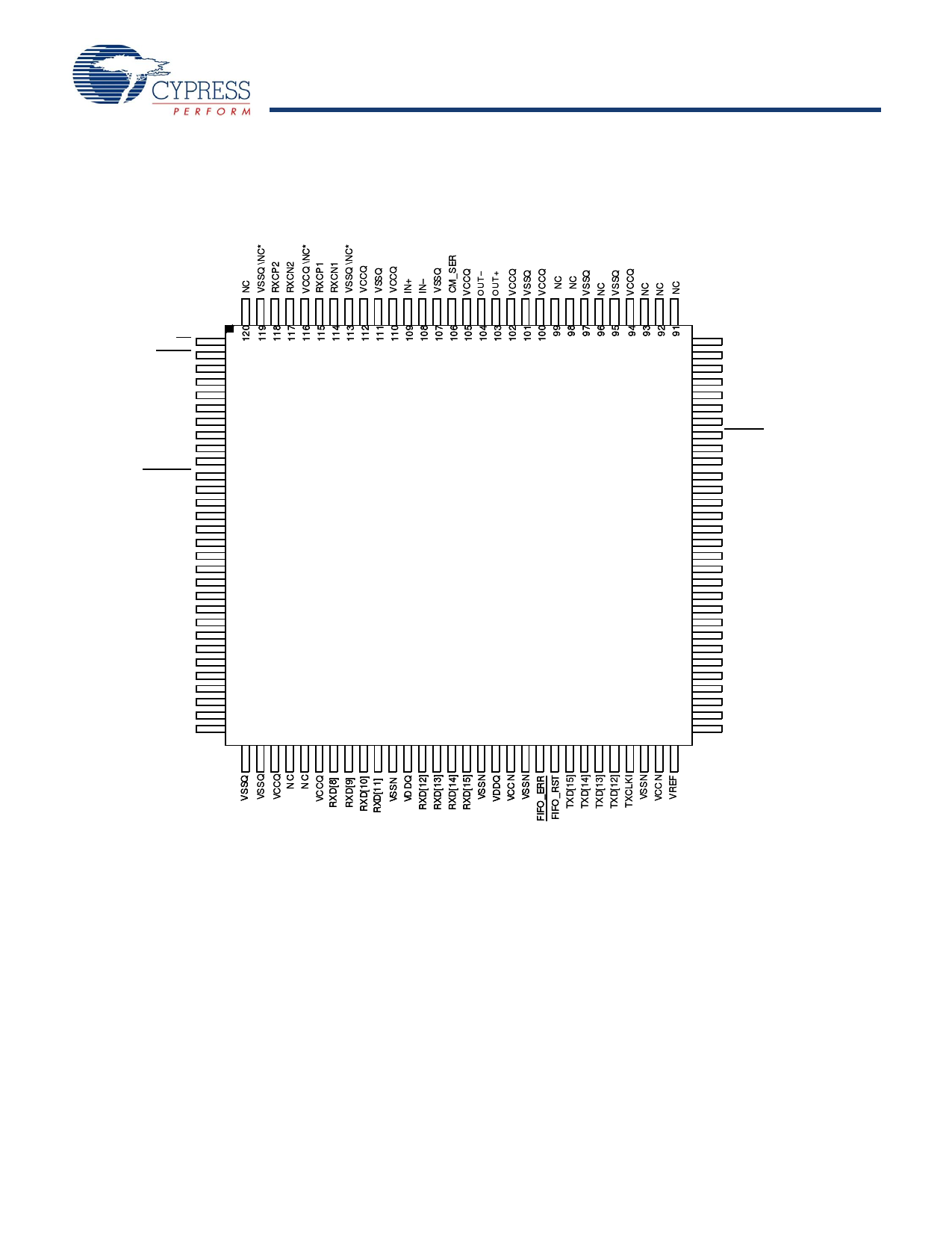
CYS25G0101DX
Pin Descriptions
CYS25G0101DX OC-48 SONET Transceiver
Pin Name I/O Characteristics
Signal Description
Transmit Path Signals
TXD[15:0]
HSTL inputs,
Parallel Transmit Data Inputs. A 16-bit word, sampled by TXCLKI↑. TXD[15] is the most
sampled by TXCLKI↑ significant bit (the first bit transmitted).
TXCLKI
HSTL Clock input
Parallel Transmit Data Input Clock. The TXCLKI is used to transfer the data into the input
register of the serializer. The TXCLKI samples the data, TXD [15:0], on the rising edge of
the clock cycle.
TXCLKO
VREF
HSTL Clock output
Input Analog
Reference
Transmit Clock Output. Divide by 16 of the selected transmit bit rate clock. It is used to
coordinate byte wide transfers between upstream logic and the CYS25G0101DX.
Reference Voltage for HSTL Parallel Input Bus. VDDQ/2.[3]
Receive Path Signals
RXD[15:0] HSTL output,
synchronous
Parallel Receive Data Output. These outputs change following RXCLK↓. RXD[15] is the
most significant bit of the output word and is received first on the serial interface.
RXCLK
HSTL Clock output Receive Clock Output. Divide by 16 of the bit rate clock extracted from the received serial
stream. RXD [15:0] is clocked out on the falling edge of the RXCLK.
CM_SER
RXCN1
Analog
Analog
Common Mode Termination. Capacitor shunt to VSS for common mode noise.
Receive Loop Filter Capacitor (Negative).
RXCN2
Analog
Receive Loop Filter Capacitor (Negative).
RXCP1
RXCP2
Analog
Analog
Receive Loop Filter Capacitor (Positive).
Receive Loop Filter Capacitor (Positive).
Device Control and Status Signals
REFCLK±
Differential LVPECL Reference Clock. This clock input is used as the timing reference for the transmit and
input
receive PLLs. A derivative of this input clock is used to clock the transmit parallel interface.
The reference clock is internally biased enabling for an AC coupled clock signal.
LFI
LVTTL output
Line Fault Indicator. When LOW, this signal indicates that the selected receive data
stream is detected as invalid by either a LOW input on SD or by the receive VCO operated
outside its specified limits.
RESET
LVTTL input
Reset for all logic functions except the transmit FIFO.
LOCKREF LVTTL input
Receive PLL Lock to Reference. When LOW, the receive PLL locks to REFCLK instead
of the received serial data stream.
SD
LVTTL input
Signal Detect. When LOW, the receive PLL locks to REFCLK instead of the received serial
data stream. The SD needs to be connected to an external optical module to indicate a
loss of received optical power.
FIFO_ERR LVTTL output
Transmit FIFO Error. When HIGH, the transmit FIFO has either under or overflowed.
When this occurs, the FIFO’s internal clearing mechanism clears the FIFO within nine clock
cycles. In addition, FIFO_RST is activated at device power up to ensure that the in and out
pointers of the FIFO are set to maximum separation.
FIFO_RST LVTTL input
Transmit FIFO Reset. When LOW, the in and out pointers of the transmit FIFO are set to
maximum separation. FIFO_RST is activated at device power up to ensure that the in and
out pointers of the FIFO are set to maximum separation. When the FIFO is reset, the output
data is a 1010... pattern.
PWRDN
LVTTL input
Device Power Down. When LOW, the logic and drivers are all disabled and placed into a
standby condition where only minimal power is dissipated.
Note
3. VREF equals to (VCC – 1.33V) if interfacing to a parallel LVPECL interface.
Document Number: 38-02009 Rev. *K
Page 5 of 17
Share Link: 