2SJ610(2002) データシートの表示(PDF) - Toshiba
部品番号
コンポーネント説明
メーカー
2SJ610 Datasheet PDF : 6 Pages
| |||
2SJ610
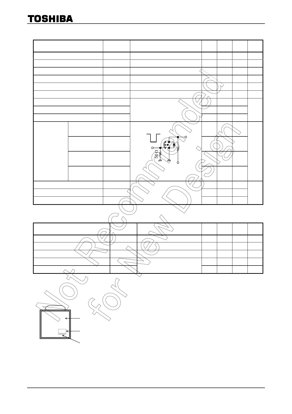
Electrical Characteristics (Tc = 25°C)
Characteristics
Gate leakage current
Drain cut-off current
Drain-source breakdown voltage
Gate threshold voltage
Drain-source ON resistance
Forward transfer admittance
Input capacitance
Reverse transfer capacitance
Output capacitance
Rise time
Switching time
Turn-on time
Fall time
Turn-off time
Total gate charge
Gate-source charge
Gate-drain charge
Symbol
Test Condition
IGSS
IDSS
V (BR) DSS
Vth
RDS (ON)
ïYfsï
Ciss
Crss
Coss
VGS = ±16 V, VDS = 0 V
VDS = -250 V, VGS = 0 V
ID = -10 mA, VGS = 0 V
VDS = -10 V, ID = -1 mA
VGS = -10 V, ID = -1.0 A
VDS = -10 V, ID = -1.0 A
VDS = -10 V, VGS = 0 V, f = 1 MHz
Min Typ. Max Unit
¾
¾
±10
mA
¾
¾ -100 mA
-250 ¾
¾
V
-1.5
¾ -3.5
V
¾
1.85 2.55
W
0.5
1.8
¾
S
¾
381
¾
¾
52
¾
pF
¾ 157 ¾
tr
10 V
VGS
ton
0V
ID = 1.0 A VOUT
¾
5
¾
¾
20
¾
RL = 100 W
ns
tf
¾
6
¾
VDD ~- 100 V
toff
Duty <= 1%, tw = 10 ms
¾
36
¾
Qg
VDD ~- -200 V, VGS = -10 V,
Qgs
ID = -2.0 A
Qgd
¾
24
¾
¾
11
¾
nC
¾
13
¾
Source-Drain Ratings and Characteristics (Tc = 25°C)
Characteristics
Continuous drain reverse current (Note 1)
Pulse drain reverse current
(Note 1)
Forward voltage (diode)
Reverse recovery time
Reverse recovery charge
Symbol
IDR
IDRP
VDSF
trr
Qrr
Test Condition
¾
¾
IDR = -2.0 A, VGS = 0 V
IDR = -2.0 A, VGS = 0 V,
dIDR/dt = 100 A/ms
Min Typ. Max Unit
¾
¾
-2.0
A
¾
¾
-4.0
A
¾
¾
2.0
V
¾
120
¾
ns
¾
540
¾
nC
Marking
J610
※
Type
※ Lot Number
Month (starting from alphabet A)
Year (last number of the christian era)
2
2002-09-11
Share Link: 