AN7208 データシートの表示(PDF) - Panasonic Corporation
部品番号
コンポーネント説明
メーカー
AN7208 Datasheet PDF : 8 Pages
| |||
ICs for FM/AM Tuner
AN7208SA
s Electrical Characteristics at VCC = 1.2 V, Ta = 25°C (continued)
Parameter
Symbol
Conditions
Min Typ
TV fIN = 221.75 MHz (continued)
Burst noise *3
VNO(TV)
Input level = 60 dBµ
Non-modulation
−1.8
FM fIN = 107.88 MHz
Conversion gain *1
Oscillation voltage
S/N *2
GCONV(FM) fOUT = 10.6 MHz
VOSC(FM) VCC = 0.95 V
S/N(FM) Input level = 60 dBµ
1 kHz 30% mod.
30 38
40 63
48 51
Quiescent current
Oscillation buffer output
Burst noise *3
ITOT(FM)
VBUF(FM)
VNO(FM)
VCC = 0.95 V
Input level = 60 dBµ
Non-modulation
7.7
66 132
−1.8
Note) Tuning is taken the peak point at 10.6 MHz output level ( VIN = 30 dBµ, non-modulation)
*1 : Conversion gain = 20 Log( ∆V (µV) ÷ 31.6)
∆V is the output difference at VIN = 30 dBµ and at VIN = 36 dBµ
*2 : Measurement is done at the detection output of the AN7233
Measure the ratio of output at fDIV = 22.5 kHz to that at fDIV = 0 Hz (modulation freq. 1 kHz)
*3 : Measurement is done at the detection output of the AN7233
Measures a peak voltage of the measurement time = within 500 ms (OK to 10 times)
Max Unit
1.8 mV[p-0]
46 dB
mV[rms]
dB
10 mA
mV[rms]
1.8 mV[p-0]
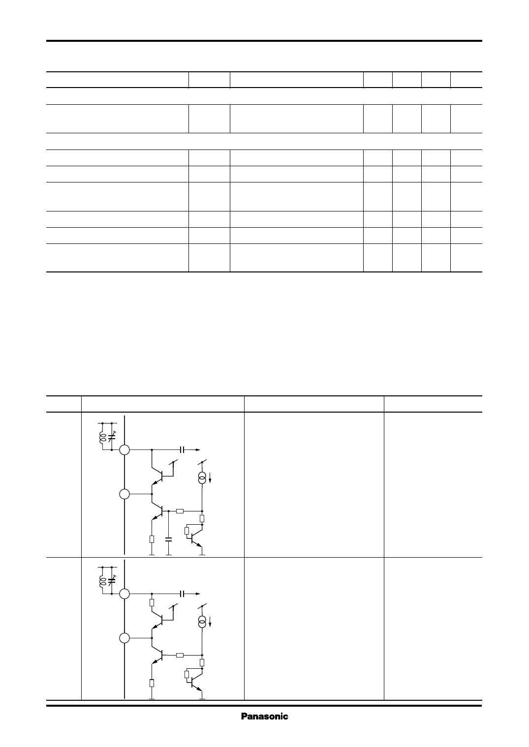
s Terminal Equivalent Circuits
Pin No.
Equivalent circuit
1
19
To mix.
Description
FM RF input
RF signal input in FM band
(Common base type)
Input resistance or pin voltage
Approx. VCC − 0.7 V
1
2
18
2
To mix.
TV RF input
RF signal input in TV band
(Common base type)
Approx. VCC − 0.7 V
3
Share Link: 