AP2201K-3.0TR データシートの表示(PDF) - BCD Semiconductor
部品番号
コンポーネント説明
メーカー
AP2201K-3.0TR Datasheet PDF : 12 Pages
| |||
Preliminary Datasheet
150mA RF ULDO REGULATOR
AP2201
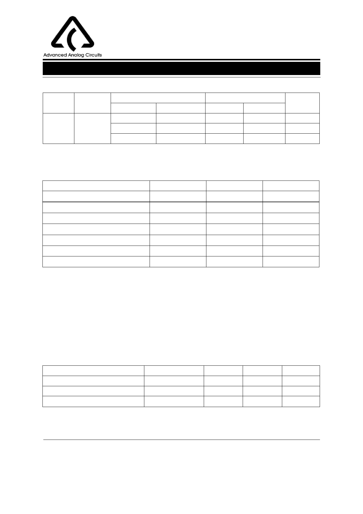
Ordering Information (Continued)
Package
SOT-23-5
Temperature
Range
-40 to 125oC
Part Number
Tin Lead
Lead Free
AP2201K-2.6TR AP2201K-2.6TRE1
AP2201K-2.8TR AP2201K-2.8TRE1
AP2201K-3.0TR AP2201K-3.0TRE1
Marking ID
Tin Lead
Lead Free
K1E
E1E
K1G
E1G
K1I
E1I
Packing Type
Tape & Reel
Tape & Reel
Tape & Reel
BCD Semiconductor's Pb-free products, as designated with "E1" suffix in the part number, are RoHS compliant.
Absolute Maximum Ratings (Note 1)
Parameter
Symbol
Value
Unit
Supply Input Voltage
Enable Input Voltage
VIN
15
V
VEN
15
V
Power Dissipation
Lead Temperature (Soldering, 5sec)
Storage Temperature
ESD (Machine Model)
PD
Internally Limited
W
TLEAD
260
oC
TSTG
-65 to 150
oC
200
V
Thermal Resistance
θJA
(Note 2)
Note 1: Stresses greater than those listed under "Absolute Maximum Ratings" may cause permanent damage to the device.
These are stress ratings only, and functional operation of the device at these or any other conditions beyond those indicated
under "Recommended Operating Conditions" is not implied. Exposure to "Absolute Maximum Ratings" for extended periods
may affect device reliability.
Note 2: Absolute maximum ratings indicate limits beyond which damage to the component may occur. Electrical specifica-
tions do not apply when operating the device outside of its operating ratings. The maximum allowable power dissipation is a
function of the maximum junction temperature, TJ(max), the junction-to-ambient thermal resistance, θJA, and the ambient tem-
perature, TA. The maximum allowable power dissipation at any ambient temperature is calculated using: PD(max)=(TJ(max) -
TA)/θJA. Exceeding the maximum allowable power dissipation will result in excessive die temperature, and the regulator will
go into thermal shutdown.
Recommended Operating Conditions
Parameter
Symbol
Supply Input Voltage
VIN
Enable Input Voltage
VEN
Operating Junction Temperature
TJ
Min
Max
Unit
2.5
13.2
V
0
13.2
V
-40
125
oC
Jun. 2005 Rev. 1. 0
BCD Semiconductor Manufacturing Limited
4
Share Link: 