AP2201K-2.6TRE1 データシートの表示(PDF) - BCD Semiconductor
部品番号
コンポーネント説明
メーカー
AP2201K-2.6TRE1 Datasheet PDF : 12 Pages
| |||
Preliminary Datasheet
150mA RF ULDO REGULATOR
AP2201
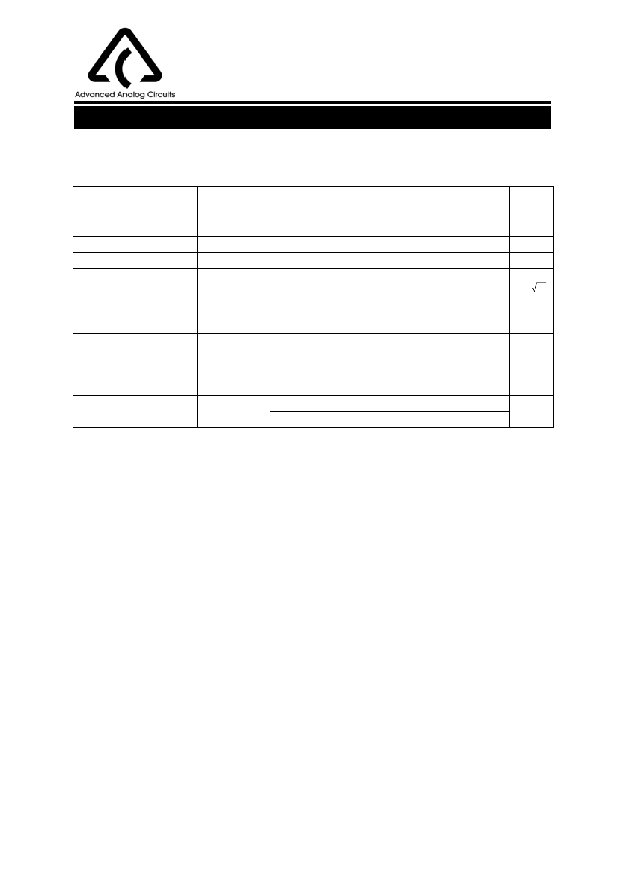
Electrical Characteristics (Continued)
VIN=VOUT +1V, IOUT = 100µA, CL = 2.2µF, VEN≥ 2.0V, TJ = 25oC, Bold typeface applies over -40oC<TJ<125oC, unless other-
wise specified.
Parameter
Symbol
Conditions
Min Typ Max Unit
Ground Pin Current (Note 6)
Ripple Rejection
Current Limit
Output Noise
(Regulator B only)
IGND
PSRR
ILIMIT
eno
VEN ≥ 2.0V, IOUT=150mA
frequency=100Hz, IOUT=100µA
VOUT = 0V
IOUT=50mA, CL=2.2µF,
470 pF from BYP to GND
1300
75
320
260
1900
µA
2500
dB
550
mA
nV / Hz
Enable Input Logic-Low
Voltage
VIL
Regulator shutdown
Enable Input Logic-High
VIH
Regulator enabled
Voltage
0.4
V
0.18
2.0
V
Enable Input Logic-Low
Current
IIL
VIL≤ 0.4V
VIL≤ 0.18V
Enable Input Logic-High
Current
IIH
VIL≥ 2.0V
VIL≥ 2.0V
0.01 -1
µA
-2
5
20
µA
25
Note 3: Output voltage temperature coefficient is defined as the worst case voltage change divided by the total temperature
range.
Note 4: Regulation is measured at constant junction temperature using low duty cycle pulse testing. Parts are tested for load
regulation in the load range from 0.1mA to 150mA. Changes in output voltage due to heating effects are covered by the thermal
regulation specification.
Note 5: Dropout voltage is defined as the input to output differential at which the output voltage drops 2% below its nominal
value measured at 1V differential.
Note 6: Ground pin current is the regulator quiescent current plus pass transistor base current. The total current drawn from the
supply is the sum of the load current plus the ground pin current.
Jun. 2005 Rev. 1. 0
BCD Semiconductor Manufacturing Limited
6
Share Link: 