APW7134 データシートの表示(PDF) - Kingbright
部品番号
コンポーネント説明
メーカー
APW7134 Datasheet PDF : 16 Pages
| |||
APW7134
Application Description (Cont.)
Input Capacitor Selection Cont.
I(Q1)
IIN
I(CIN)
Q1
L
VIN
CIN
I(L)
Q2
COUT
I(COUT)
IOUT
PWM
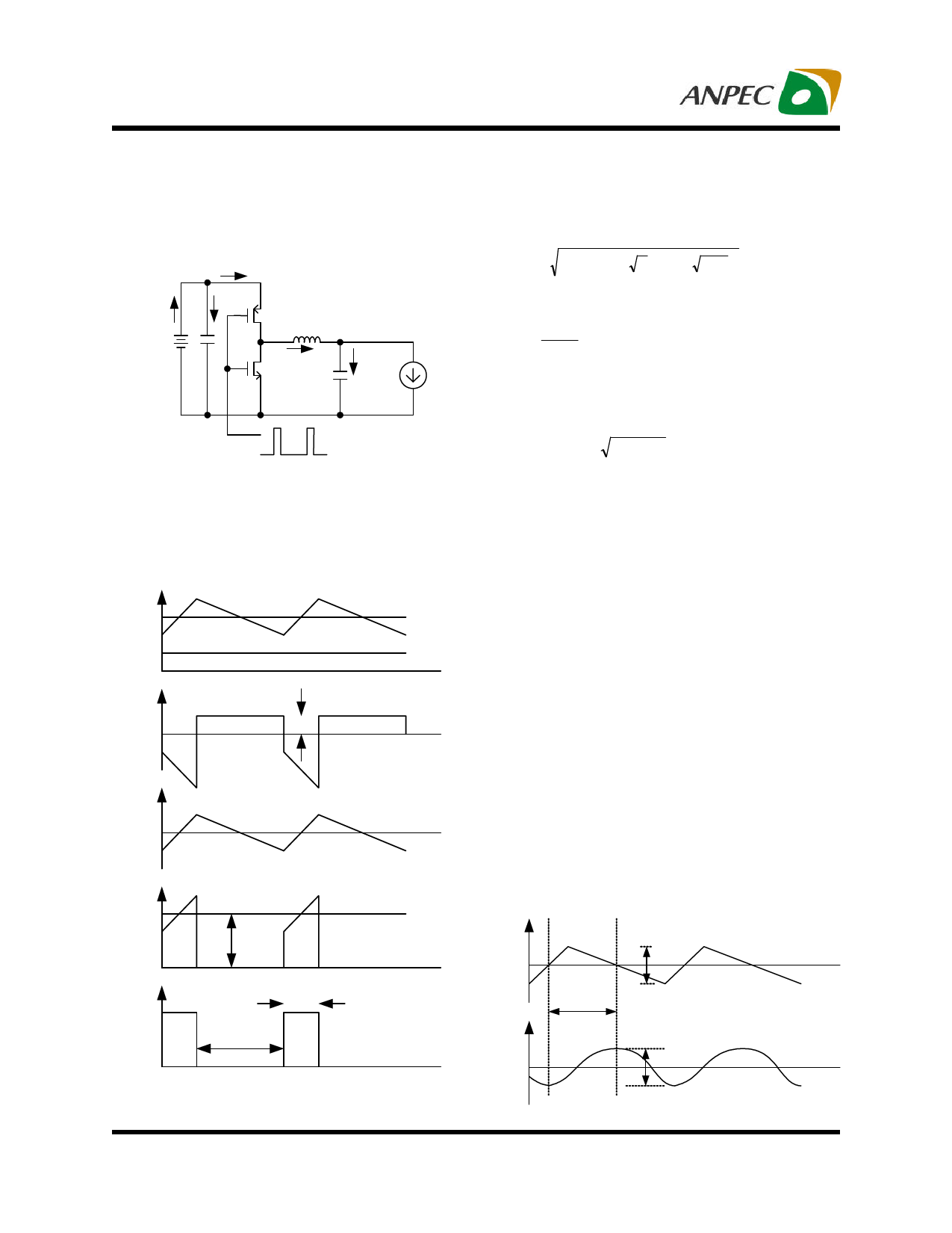
Figure-1
Figure-1 shows a schematic of a Buck structure. The
waveforms show as Figure-2.
Observe the waveform of I(CIN),the RMS value of I(CIN) is
[ ] ( ) ( ) ( ) I CIN =
IOUT −IIN 2 ⋅
2
D + IIN ⋅
2
1−D
(2)
Replace D and IIN by following relation:
D = VOUT
(3)
VIN
IIN = D⋅IOUT
(4)
The RMS value of input capacitor current equal:
( ) I CIN = IOUT ⋅ D(1 − D) )
(5)
When D=0.5 the RMS current of input capacitor will
be maximum value. Use this value to choose the
input capacitor with suitable current rating.
Output Capacitor Selection
IL
The output voltage ripple is a significant parameter to
IOUT
estimate the performance of a convertor. There are
two discrete components that affect the output
0A
IIN
voltage ripple bigger or smaller. It is recommended to
use the criterion has mentioned above to choose a
suitable inductor. Then based on this known inductor
0A
IIN
I(CIN)
current ripple condition, the value and properties of
output capacitor will affect the output voltage ripple
better or worse. The output voltage ripple consists of
two portions, one is the product of ESR and inductor
0A
current ripple, the other portion is a function of the
I(COUT)
inductor current ripple and the output capacitance.
Figure-3 shows the waveforms to explain the part
I(Q1)
decided by the output capacitance.
IOUT
0A
D*TS
(1-D)*TS
0A
PWM
Figure-2
Copyright © ANPEC Electronics Corp.
Rev. A.1 - Aug., 2006
0A
∆IL
I(COUT)
0.5TS
∆VOUT1
VOUT
Figure-3
11
www.anpec.com.tw
Share Link: 