APW7134 データシートの表示(PDF) - Kingbright
部品番号
コンポーネント説明
メーカー
APW7134 Datasheet PDF : 16 Pages
| |||
APW7134
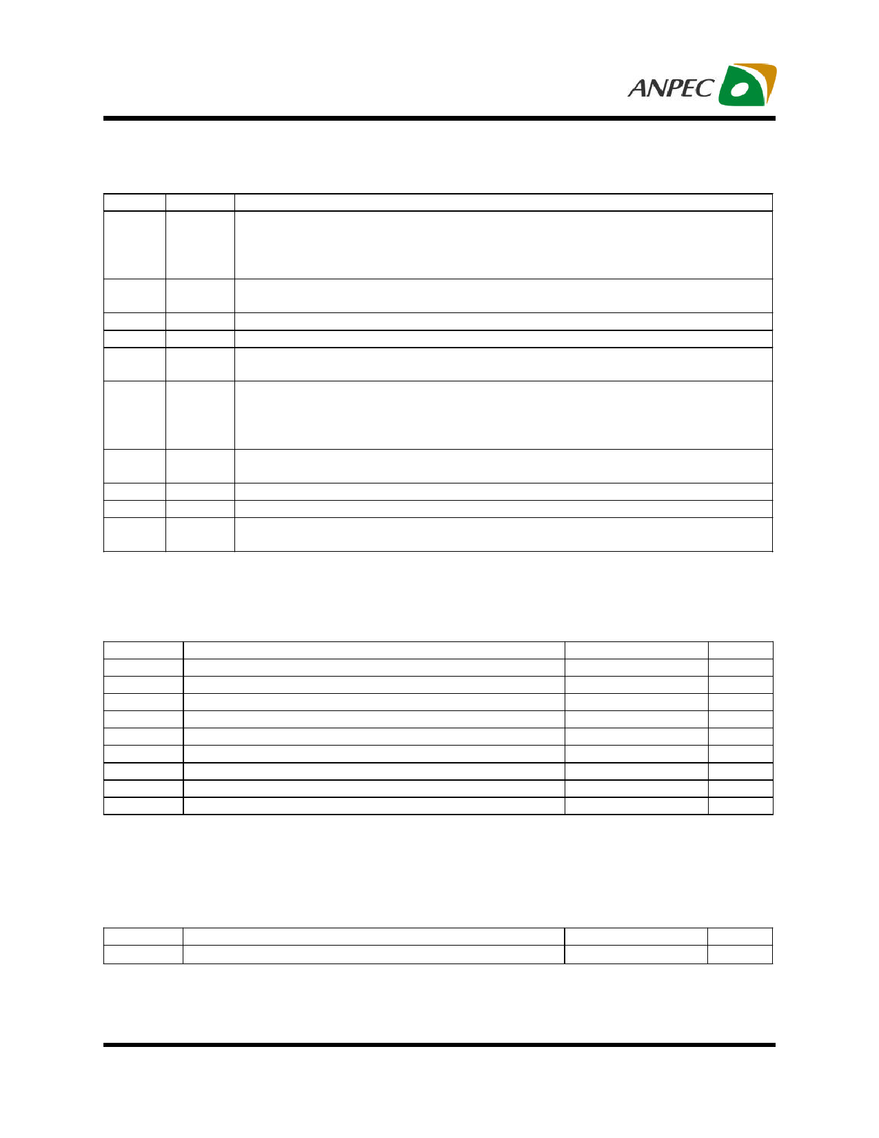
Pin Description
Pin No.
1
2
3
4
5
6
7
8
9
10
Name
EN1
FB1
IN2
GND2
SW2
EN2
FB2
IN1
GND1
SW1
Function
Channel 1 Enable Control Input. Drive EN1 above 1.5V to turn on the Channel 1.
Drive EN1 below 0.3V to turn it off. In shutdown situation, all functions are disabled
to decrease the supply current below 1µA.There is no pull high or pull low ability
inside.
Channel 1 Feedback Input. Connect FB1 to the center point of the external resistor
divider. The feedback voltage is 0.6V.
Channel 2 Supply Input. Bypass to GND with a 4.7µF or greater ceramic capacitor.
Ground 2. Connected the exposed pad to GND2.
Channel 2 Power Switch Output. Inductor connection to drains of the internal
PMOSFET and NMOSFET switches.
Channel 2 Enable Control Input. Drive EN2 above 1.5V to turn on the Channel 2.
Drive EN2 below 0.3V to turn it off. In shutdown situation, all functions are disabled
to decrease the supply current below 1µA.There is no pull high or pull low ability
inside.
Channel 2 Feedback Input. Connect FB2 to the center point of the external resistor
divider. The feedback voltage is 0.6V.
Channel 1 Supply Input. Bypass to GND with a 4.7µF or greater ceramic capacitor.
Ground 1. Connected the exposed pad to GND1.
Channel 1 Power Switch Output. Inductor connection to drains of the internal
PMOSFET and NMOSFET switches.
Absolute Maximum Ratings
Symbol
VIN1/IN2
VFB1/FB2
VEN1/EN2
VSW1/SW2
ISW_PEAK
TJ
TSTG
TSDR
VESD
Parameter
Input Supply Voltage (IN1/IN2 to GND1/GND2)
Voltage on FB1 and FB2
Voltage on EN1 and EN2
Voltage on SW1 and SW2
Peak SW Current
Junction temperature
Storage temperature
Soldering temperature, 10 seconds
Minimum ESD rating (Human body mode) (Note 1)
Note 1: The device is ESD sensitive. Handling precautions are recommended.
Value
-0.3 ~ 6
-0.3 ~ VIN1/IN2+0.3
-0.3 ~ VIN1/IN2+0.3
-0.3 ~ VIN1/IN2+0.3
1.3
150
-65 ~ 150
300
±3
Unit
V
V
V
V
A
°C
°C
°C
KV
Thermal Characteristics
Symbol
Parameter
θJA Junction-to-Ambient Resistance in free air (Note 2)
Note 2: θJA is measured on approximately 1¨ square of 1 oz copper.
Value
50
Unit
°C/W
Copyright © ANPEC Electronics Corp.
3
Rev. A.1 - Aug., 2006
www.anpec.com.tw
Share Link: 