Q67100-Q1331 データシートの表示(PDF) - Siemens AG
部品番号
コンポーネント説明
メーカー
Q67100-Q1331 Datasheet PDF : 22 Pages
| |||
HYB 39S16400/800/160AT-8/-10
16 MBit Synchronous DRAM
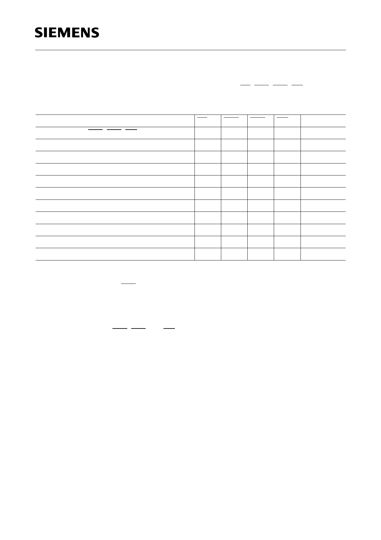
Operation Definition
All of SDRAM operations are defined by states of control signals CS, RAS, CAS, WE, and DQM at
the positive edge of the clock. The following list shows the most important operation commands.
Operation
CS RAS CAS WE (L/U)DQM
Standby, Ignore RAS, CAS, WE and Address H
X
X
X
X
Row Address Strobe and Activating a Bank
L
L
H
H
X
Column Address Strobe and Read Command L
H
L
H
X
Column Address Strobe and Write Command L
H
L
L
X
Precharge Command
L
L
H
L
X
Burst Stop Command
L
H
H
L
X
Self Refresh Entry
L
L
L
H
X
Mode Register Set Command
L
L
L
L
X
Write Enable/Output Enable
X
X
X
X
L
Write Inhibit/Output Disable
X
X
X
X
H
No Operation (NOP)
L
H
H
H
X
Mode Register
For application flexibility, a CAS latency, a burst length, and a burst sequence can be programmed
in the SDRAM mode register. The mode set operation must be done before any activate command
after the initial power up. Any content of the mode register can be altered by reexecuting the mode
set command. Both banks must be in precharged state and CKE must be high at least one clock
before the mode set operation. After the mode register is set, a Standby or NOP command is
required. Low signals of RAS, CAS, and WE at the positive edge of the clock activate the mode set
operation. Address input data at this timing defines parameters to be set as shown in the following
table.
Semiconductor Group
9
1998-10-01
Share Link: 