CS3524A データシートの表示(PDF) - Cherry semiconductor
部品番号
コンポーネント説明
メーカー
CS3524A Datasheet PDF : 6 Pages
| |||
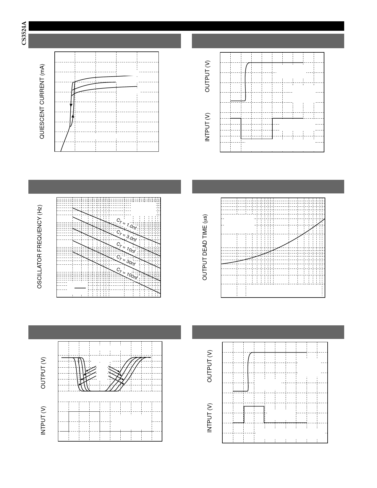
Typical Performance Characteristics continued
Quiescent Supply Current vs. Supply Voltage Over
Temperature
10
Shutdown Delay From PWM Comparator
9
8
TA = -55°C
7
TA = 25°C
6
TA = 125°C
5
4
3
2
Note: Outputs off. RT = ∞
1
0
0
10
20
30
40
50
SUPPLY VOLTAGE VIN (V)
20
OUTPUT at
15
VOA or VOB
10
5
VIN = 20V
RL = 2kΩ
0
TA = 25˚C
5
4
3
INPUT at VOB
2
1
0
Note: Minimum input pulse width
to latch is 200ns
0
1
2
3
DELAY TIME (µs)
Oscillator Frequency vs. Timing Components Resistor
Over Timing Capacitance
1M
VIN = 20V
TA = 25˚C
100k
10k
1k
CT = 1.0nf
CT = 3.0nf
CT = 10nf
CT = 30nf
CT = 100nf
100
1
f≈
1.15
RTCT
2
5
10 20
50 100
TIMING RESISTOR - RT (kΩ)
Output Dead Time vs. Timing Capacitor Value
10
5.0
VIN = 20V
RT = 2700Ω
TA = 25˚C
2.0
1.0
0.5
0.2
0.1
1
Note: Dead time = osc output pulse
width plus output delay
2
5
10 20
50 100
TIMING CAPACITOR - CT (nf)
Current Limit Amplifier Delay
OUTPUT at COMP
6
5
Overdrive
4
5%
10%
3
20%
2
50%
1
0
INPUT at ISENSE+
0.2
0.1
VIN 20V TA 25˚C
EA+ = VREF
ISENSE– = Gnd
0.0
0
1
2
3
4
DELAY TIME (µs)
Turn-Off Delay From Shutdown
20
15
VIN = 20V
RL = 2kΩ
10
TA = 25˚C
5
OUTPUT at
VOA OR VOB
0
1.0
0.5
INPUT at
SHUTDOWN
0.0
Note: Minimum input pulse width
to latch is 200ns
0
1
2
3
DELAY TIME (µs)
4
Share Link: 